Samsung Foundry Strengthens IP... Supports AI and Automotive Customers
3 Major IP Partners and Dozens of IPs Secured
Cutting-Edge IP Strategy Unveiled at SAFE Forum
Expansion of Cooperation with Domestic IP Partners Also Announced
Samsung Electronics has partnered with semiconductor intellectual property (IP) companies to enhance its foundry (semiconductor contract manufacturing) competitiveness. By securing IP optimized for its own processes, the company aims to attract new fabless (semiconductor design) customers and strengthen development support capabilities for all clients. It also announced plans to unveil related IP strategies at the 'Samsung Advanced Foundry Ecosystem (SAFE) Forum' to be held in the United States this month.
Samsung Electronics' Foundry Business Division announced on the 14th that it will expand its IP portfolio and build related ecosystems through collaboration with next-generation IP partners such as Synopsys, Cadence, and Alphawave Semi.
Semiconductor IP is a design block that implements specific semiconductor functions as circuits. Utilizing IP in semiconductor chip design enables the creation of high-performance products quickly and easily. IP partners develop IP and provide it to fabless companies, foundries, and integrated device manufacturers (IDMs), receiving license fees in return. Synopsys, Cadence, and Alphawave Semi together hold over 80% of the global IP market share.
Going forward, Samsung Electronics will provide foundry process information necessary for developing cutting-edge IP, such as process design kits (PDK) and design methodologies (DM), to IP partners. These partners will use the information to develop Samsung Foundry process-optimized IP, which will be offered to domestic and international fabless customers planning to manufacture products at Samsung Foundry.

Securing IP for Various Applications Including AI and GPU... Strengthening Competitiveness in Automotive Sector
Through this collaboration, Samsung Electronics will secure core IPs required by customers across all fields, including artificial intelligence (AI), graphics processing units (GPU), high-performance computing (HPC), as well as automotive and mobile sectors. It will acquire dozens of IPs usable from 3-nanometer (nm; 1 nm = one billionth of a meter) to 8 nm processes.
Samsung will also prepare advanced interface IPs enabling high-speed data input/output and package-related UCIe (Universal Chiplet Interconnect Express) IPs, which prevent compatibility issues between different chips, such as chiplets (technology that integrates multiple semiconductors into a single package). In the automotive sector, it plans to secure IPs that meet the highest quality standards for automotive semiconductors to enhance competitiveness.
In this case, fabless customers producing products at Samsung Foundry will be able to timely utilize IP optimized for relevant processes according to their product development stages. This reduces errors from the early design phase and cuts down the time and cost required for prototype production, verification, and mass production. Samsung Electronics explains that the time from chip development to mass production can be shortened from the existing 3.5?5 years to 1.5?2 years.
Shin Jong-shin, Vice President of Samsung Electronics' Foundry Business Division, said, "Samsung Electronics prioritizes customer success and is expanding its cutting-edge IP portfolio. We will continue to expand cooperation not only with global IP partners but also with domestic IP partners to support customers' innovative product development and mass production more easily and quickly."
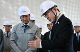
![Samsung SAFE Forum Ecosystem Guide Image / [Image Source=Samsung Electronics Semiconductor Newsroom]](http://www.asiae.co.kr/news/img_view.htm?img=2023061411074563281_1686708465.png)
Samsung SAFE Forum Ecosystem Guide Image / [Image Source=Samsung Electronics Semiconductor Newsroom]
View original image"Cutting-edge IP Roadmap to be Unveiled at This Month's SAFE Forum"
Samsung Electronics currently collaborates with 56 IP partners and provides over 4,000 IPs to customers. Since the launch of the Foundry Business Division in 2017, the number of IP partners and IPs has steadily increased, resulting in a threefold expansion of the IP scale. Because fabless companies cannot independently secure all IPs needed for semiconductor product development, Samsung secures widely used IPs to enhance its development support capabilities for customers.
Last year, the number of Samsung Foundry customers more than doubled compared to 2017. Samsung Electronics is striving to secure customers based on stable yields in advanced processes. It announced cooperation with the U.S. AI semiconductor design company Ambarella and is expanding its customer base into mobile, AI, HPC, and automotive sectors.
Hot Picks Today
 As Samsung Falters, Chinese DRAM Surges: CXMT Returns to Profit in Just One Year
- "Most Americans Didn't Want This"... Americans Lose 60 Trillion Won to Soaring Fuel Costs
- Man in His 30s Dies After Assaulting Father and Falling from Yongin Apartment
- Samsung Union Member Sparks Controversy With Telegram Post: "Let's Push KOSPI Down to 5,000"
- "Why Make Things Like This?" Foreign Media Highlights Bizarre Phenomenon Spreading in Korea
At the SAFE Forum to be held on the 28th (local time) in San Jose, USA, Samsung Electronics plans to disclose detailed cooperation with IP partners and unveil its cutting-edge IP roadmap and strategy. The SAFE Forum is Samsung Electronics' annual event introducing new technologies and strategies with various foundry ecosystem partners, including electronic design automation (EDA), IP, semiconductor assembly and test outsourcing (OSAT), and design solution partners (DSP).
© The Asia Business Daily(www.asiae.co.kr). All rights reserved.