Ministry of Industry Holds System Semiconductor Strategy Meeting... Discussing Ecosystem Strengthening Measures Including Design and Back-end Processes
On the 16th, the Ministry of Trade, Industry and Energy held a system semiconductor export and investment strategy meeting with semiconductor industry officials as a follow-up to the 'National Advanced Industry Promotion Strategy' announced the previous day. They announced the 'System Semiconductor Ecosystem Strengthening Implementation Strategy,' aiming to become a leading country in system semiconductors based on the world's largest cluster and an organic ecosystem, and discussed tasks to enhance the competitiveness of system semiconductors.

System semiconductors, which account for 60% of the semiconductor market, are the core of industrial and security supply chains in the era of artificial intelligence and electrification. However, compared to Korea's world-leading memory semiconductors, the global market share of system semiconductors is only about 3%, indicating low competitiveness. Meeting participants shared the recognition that, amid a trend of specialization in each field of the system semiconductor value chain such as IP-design-design house-foundry-post-processing according to product and technology advancement, Korea must leverage its strengths to compensate for its weaknesses.
In Korea’s world-class advanced manufacturing sector, it is necessary to enhance competitiveness through facility and technology investments to respond to the investment competition and strengthen the foundry ecosystem including design houses and IP. It is also essential to supplement the overall industrial ecosystem competitiveness in areas pointed out as weaknesses, such as semiconductor design technology and companies, post-processing, and specialized personnel.
The Ministry of Trade, Industry and Energy’s follow-up strategy to strengthen the system semiconductor ecosystem includes ▲establishing the world’s largest ‘semiconductor cluster,’ ▲upgrading ecosystem competitiveness across design, manufacturing, and post-processing, ▲supporting large-scale core technology development for next-generation semiconductors, ▲strengthening semiconductor growth foundations such as tax and finance and excellent human resources, and ▲supporting overseas technology cooperation and exports in response to supply chain restructuring.
In particular, to upgrade the ecosystem across design, manufacturing, and post-processing, the plan is to expand the opening of foundries for prototype production and mass production targeting domestic fabless companies’ multi-demand processes such as 4nm processes for AI semiconductors and legacy processes for automotive and home appliance semiconductors. A private-led investment of 2 trillion KRW will be made for innovation cooperation in the foundry-materials-parts-equipment-fabless ecosystem, including R&D, prototyping, and human resources.
Additionally, within this month, 20 promising star fabless companies in fields such as AI, power, and sensors will be selected, and company-led dedicated R&D, design tools-IP-development-prototype-sales channels will be supported in an integrated manner to foster them into global companies. For fabless companies, support will be provided at about twice the level of existing general processes for prototype production in advanced processes to reduce their cost burden.
They also discussed attracting 24 trillion KRW in private investment outside the metropolitan area to establish packaging R&D and production bases, and promoting large-scale technology development projects to support the development and commercialization of post-processing materials-parts-equipment and packaging technologies. A preliminary feasibility study application of 360 billion KRW is expected in the second half of this year.
Considering the recently deteriorated investment environment, there was also discussion on promptly concentrating investment in the already established fabless fund and creating a new fund by the first half of next year to support investments as soon as the current fund is exhausted. Through the fund, focused investments will be made in technology development, commercialization, marketing, and mergers and acquisitions (M&A) of small and medium-sized enterprises and startups in design fields such as AI semiconductors, power semiconductors, IP companies, and design houses, significantly contributing to corporate growth.
Hot Picks Today
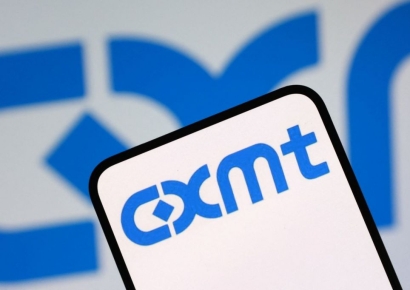 As Samsung Falters, Chinese DRAM Surges: CXMT Returns to Profit in Just One Year
- "Most Americans Didn't Want This"... Americans Lose 60 Trillion Won to Soaring Fuel Costs
- Man in His 30s Dies After Assaulting Father and Falling from Yongin Apartment
- Samsung Union Member Sparks Controversy With Telegram Post: "Let's Push KOSPI Down to 5,000"
- "Why Make Things Like This?" Foreign Media Highlights Bizarre Phenomenon Spreading in Korea
Meanwhile, KOTRA, which attended the meeting, introduced projects to intensively support North American market entry for fabless and materials-parts-equipment semiconductor companies, including ▲establishing local entry support bases and ▲demand-based B2B cooperation support projects. Within this year, a new GP (Global Partnering) Center will be opened in Austin, USA, where global semiconductor manufacturing plants are located, to support local market entry (permits, environmental regulations, etc.) and marketing for domestic materials-parts-equipment companies. They also announced plans to hold demand consultation meetings for promising domestic small and medium semiconductor companies entering the U.S. market to support B2B cooperation.
© The Asia Business Daily(www.asiae.co.kr). All rights reserved.