US AMAT unveils new electron beam technology... "First full-process research lab in Korea"
US Semiconductor Equipment Company 'Applied Materials'
Reveals TFE Technology and Equipment Emitting Electron Beams at Room Temperature
Pre-Process R&D Center Announced... "First Global Business Site"
[Asia Economy Reporter Kim Pyeonghwa] As semiconductor processes become increasingly complex, electron beam (eBeam) technology, which detects and classifies defects during manufacturing, is gaining attention. Applied Materials (AMAT), a global semiconductor equipment company, recently introduced new technology to expand its presence in the electron beam market. In the process of expanding its business in Korea, it will unveil its first front-end process research and development (R&D) center among its global sites.
Applied Materials Korea held a press briefing on the 13th at the Grand Intercontinental Seoul Parnas in Seoul. The event was to introduce the electron beam imaging innovation technology and new equipment products, which were globally unveiled last December, to the domestic market.
Applied Materials announced that it has commercialized 'Cold Field Emission (CFE)' to innovate electron beam imaging technology. They also shared news of launching two electron beam systems based on CFE technology: 'SEM Vision G10' and 'Prime Vision 10.'

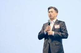
Park Kwang-sun, President of Applied Materials Korea, is giving a presentation at the meeting. /
Electron beam systems detect and classify defects occurring during semiconductor chip production by shooting electrons. Although the detection area is smaller than that of optical systems, which use light projected through lenses, the image resolution is higher. This makes it easier to identify defects, making electron beam systems highly useful in complex fine processes.
Applied Materials introduced a new technology called CFE in electron beam systems, which were previously based on Thermal Field Emission (TFE). While TFE emits electron beams at high temperatures above 1500 degrees Celsius, CFE emits electron beams at room temperature. CFE offers 50% higher resolution than TFE and processes images ten times faster at the same resolution.
Lee Seok-woo, Head of Technology at Applied Materials Korea, explained, "CFE has existed theoretically for 30 to 40 years but had not been commercialized due to technological limitations until we became the first in the industry to introduce it. The CFE electron beam system can accelerate the development and production of next-generation processes such as Gate-All-Around (GAA) logic chips, highly integrated DRAM, and 3D NAND memory."
![Comparison image of Thermionic Field Emission (TFE) and Cold Field Emission (CFE) electron beams / [Image courtesy of Applied Materials Korea]](http://www.asiae.co.kr/news/img_view.htm?img=2023021314591022210_1676267950.jpg)
Comparison image of Thermionic Field Emission (TFE) and Cold Field Emission (CFE) electron beams / [Image courtesy of Applied Materials Korea]
View original imageApplied Materials launched the 'SEM Vision G10' in December last year using CFE technology. SEM Vision G10 is a review tool that inspects defects occurring during semiconductor manufacturing and can be used across the semiconductor industry. It began supplying some customers during its development in 2020 and has generated over $400 million in sales to date. Another newly launched device is the 'Prime Vision 10,' which features 3D inspection technology to detect micro-defects on wafer surfaces.
Applied Materials anticipates that as semiconductor demand grows and the industry expands, manufacturing processes will become more complex. The use of advanced electron beam systems will inevitably increase. In fact, the global electron beam market grew by 95% between 2019 and 2021, a growth rate that stands out compared to the 68% growth of the overall semiconductor equipment and wafer-inclusive WEF market during the same period. Applied Materials holds the top position in the electron beam market with a 50% market share.
![SEM Vision G10 Equipment Image / [Image provided by Applied Materials Korea]](http://www.asiae.co.kr/news/img_view.htm?img=2023021314591722211_1676267957.jpg)
Applied Materials plans to expand its electron beam business and strengthen its presence in the semiconductor equipment market. As part of this, it will establish an R&D center in Korea. In July last year, it signed a memorandum of understanding (MOU) with Gyeonggi Province and the Ministry of Trade, Industry and Energy to establish the R&D center and is currently working on site selection. A follow-up announcement regarding investment scale and other details will be made soon.
Park Kwang-sun, President of Applied Materials Korea, said, "Building a front-end process research center overseas is the first priority. There are no such cases in Taiwan or Europe, nor are there plans for the near future." He added, "Establishing a front-end research center in Korea will enable organic collaboration with Korean customers (Samsung Electronics, SK Hynix). It is meaningful because it creates a platform for cooperation across foundry and memory semiconductor businesses, and we are pushing forward with its establishment."
Hot Picks Today
 "With This Certificate, Even Those in Their 60s...
- Popcorn Container Craze at Theaters Sparks Sell-Out Frenzy, Emerges as New Reven...
- When His Father Suddenly Collapsed Before His Eyes... 13-Year-Old Son Preserves ...
- Female Game Caster Makes Bold Move After Criticism Over "Short Skirt" on Broadca...
- "Quit Office Job to Earn Over 200 Million Won a Year"… Chinese Woman in Her 30s...
![Lee Seok-woo, Head of Technology at Applied Materials Korea, is giving a presentation. / <br>[Photo by Applied Materials Korea]](http://www.asiae.co.kr/news/img_view.htm?img=2023021314592722212_1676267967.jpeg)
Lee Seok-woo, Head of Technology at Applied Materials Korea, is giving a presentation. /
[Photo by Applied Materials Korea]
Applied Materials is the world's leading semiconductor equipment company headquartered in Silicon Valley, USA. Last year, Korea accounted for 17% of its total revenue ($25.79 billion). The Korean subsidiary was established in 1989 and employs over 2,100 people.
© The Asia Business Daily(www.asiae.co.kr). All rights reserved.


!["They Said It Was 'Delicious' Milk... Is the 'List of Fake Milk Products in Korea' for Real? [Matjal X-File]"](https://cwcontent.asiae.co.kr/asiaresize/307/2023072413274517286_1690172865.jpg)