Samsung Foundry "To Complete Preparation for Mass Production of 2nm Automotive Products by 2026"
Next-Generation 'eMRAM' 5nm Plan for Vehicles Announced
Leading the Future Car Era with Customized Mass Production to Meet Customer Demands
Samsung Electronics has unveiled its foundry (semiconductor contract manufacturing) business vision in Europe, the global hub of the automotive industry. The company plans to complete preparations for mass production of 2-nanometer (nm; 1 nm equals one billionth of a meter) automotive solutions by 2026 and expand its next-generation vehicle product portfolio to enhance business competitiveness.
On the 19th (local time), Samsung Electronics held the 'Samsung Foundry Forum 2023' in Munich, Germany. Following its participation in the world's largest motor show (IAA) held in Munich last month, the company hosted a related event directly in Germany, a key European market, to expand cooperation with European customers and strengthen its partner position in the automotive sector.

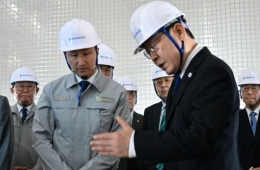
Choi Si-young, President of Samsung Electronics Foundry Business Division, delivering the keynote speech at the 'Samsung Foundry Forum 2023' held last July at COEX, Samseong-dong, Seoul / Photo by Samsung Electronics
View original imageAt the event, the company unveiled an advanced process roadmap and foundry strategies tailored to various applications. It introduced a range of customized solutions from 2-nanometer processes to legacy processes based on 8-inch wafers. Samsung Advanced Foundry Ecosystem (SAFE) partners shared technology trends and development directions through booth exhibitions.
Choi Si-young, President of Samsung Electronics Foundry Business Division, said, "We plan to timely develop processes optimized for the automotive semiconductor market and mass-produce AI semiconductors for autonomous driving stages, power semiconductors, and microcontroller units (MCUs) tailored to customer demands." He added, "With differentiated foundry solutions, we will lead the era of electric and autonomous vehicles."
Next-Generation Automotive Memory Product Mass Production Portfolio Established
Samsung Electronics plans to complete preparations for mass production of cutting-edge 2-nanometer automotive solutions by 2026. The company will also expand its portfolio of next-generation embedded Magnetic Random Access Memory (eMRAM) and 8-inch BCD processes (used in power semiconductor production).
eMRAM is a next-generation automotive memory semiconductor that operates stably at high temperatures based on fast read/write speeds. Samsung Electronics was the first in the industry to mass-produce products equipped with 28-nanometer-based eMRAM in 2019. Currently, it is developing 14-nanometer eMRAM based on FinFET processes, targeting 2024. In 2026 and 2027, the company plans to raise mass production levels with 8-nanometer and 5-nanometer eMRAM processes. The 8-nanometer eMRAM is expected to improve integration density by 30% and speed by 33% compared to the previous 14-nanometer product.
Samsung Electronics will expand its mass-produced 130-nanometer automotive BCD process to 90 nanometers by 2025. The 90-nanometer automotive BCD process can reduce chip area by about 20% compared to the 130-nanometer process. The company also plans to increase the high voltage applied to automotive solutions from 70 volts (V) to 120 V through power semiconductor performance enhancement technology. The process design kit (PDK) applying 120 V to the 130-nanometer BCD process will be provided in 2025.
![The scene at the 'Samsung Foundry Forum 2023' held last July at COEX, Samseong-dong, Seoul / [Photo by Samsung Electronics]](http://www.asiae.co.kr/news/img_view.htm?img=2023070416024886199_1688454168.jpg)
The scene at the 'Samsung Foundry Forum 2023' held last July at COEX, Samseong-dong, Seoul / [Photo by Samsung Electronics]
View original imageStrengthening Foundry Technology through Advanced Package Consortium
Samsung Electronics will lead an advanced package consortium to develop differentiated 2.5D and 3D package solutions tailored to applications such as automotive and high-performance computing (HPC). To this end, the company has established the 'MDI Alliance,' an advanced package consortium with 20 partners including SAFE partners as well as memory, package substrate, and test specialized companies.
Hot Picks Today
 As Samsung Falters, Chinese DRAM Surges: CXMT Returns to Profit in Just One Year
- "Most Americans Didn't Want This"... Americans Lose 60 Trillion Won to Soaring Fuel Costs
- Man in His 30s Dies After Assaulting Father and Falling from Yongin Apartment
- Samsung Union Member Sparks Controversy With Telegram Post: "Let's Push KOSPI Down to 5,000"
- "Why Make Things Like This?" Foreign Media Highlights Bizarre Phenomenon Spreading in Korea
Meanwhile, prior to the event in Germany, Samsung Electronics held the same events in the United States (June), Korea (July), and Japan (October). For global customers unable to attend the offline events, related content will be made available on Samsung Electronics Semiconductor website from the 2nd of next month until the end of the year.
© The Asia Business Daily(www.asiae.co.kr). All rights reserved.