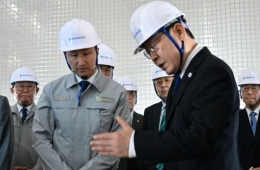
Moon Seung-wook: "Comprehensive Measures for the 'System Semiconductor Packaging Industry' to Be Prepared in the First Half of Next Year"
Visit to the 220 Billion KRW Advanced Semiconductor Packaging Investment Site

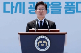
Moon Seung-wook, Minister of Trade, Industry and Energy. (File photo)
Photo by Yonhap News
[Asia Economy Reporter Joo Sang-don] Moon Seung-wook, Minister of Trade, Industry and Energy, stated on the 7th, "We will prepare comprehensive measures to expand the base of the system semiconductor packaging industry by the first half of next year by gathering opinions from industry, academia, and research institutes."
Minister Moon made these remarks while attending the 'Nepes Rawe Cheongan Campus Completion Ceremony' held at the advanced industrial complex in Goesan, Chungbuk on the same day.
The Cheongan Campus is the world's first 600mm PLP mass production fabless company invested 220 billion KRW by Nepes Rawe (a subsidiary of Nepes), a system semiconductor packaging company. It applies advanced packaging technology that can produce five times more semiconductor chips at once compared to the existing WLP method, which packages wafers without cutting them into chip units, securing production efficiency and price competitiveness.
Hot Picks Today
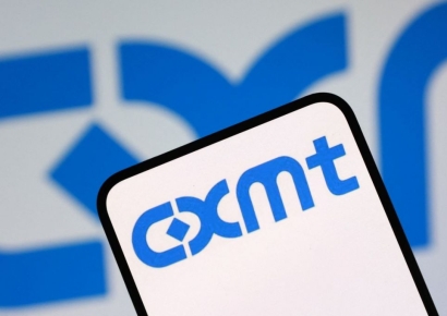 As Samsung Falters, Chinese DRAM Surges: CXMT Returns to Profit in Just One Year
- "Most Americans Didn't Want This"... Americans Lose 60 Trillion Won to Soaring Fuel Costs
- Man in His 30s Dies After Assaulting Father and Falling from Yongin Apartment
- Samsung Union Member Sparks Controversy With Telegram Post: "Let's Push KOSPI Down to 5,000"
- "Why Make Things Like This?" Foreign Media Highlights Bizarre Phenomenon Spreading in Korea
Minister Moon said, "The government will spare no support to ensure our packaging industry achieves remarkable results," adding, "We will promote the large-scale preliminary feasibility study project for the advanced packaging platform announced in the 'K-Semiconductor Strategy' last May within this year."
© The Asia Business Daily(www.asiae.co.kr). All rights reserved.