Lee Jae-yong "Design Revolution Once Again"... Company-wide Integrated 'Design Strategy Meeting' Held
Visit to Seoul R&D Campus... Resumption of Management Activities

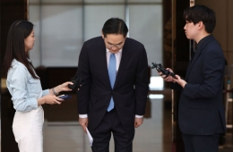
Samsung Electronics Vice Chairman Lee Jae-yong (second from the left) is holding a design strategy meeting on the 12th at the Seoul R&D Campus located in Umyeon-dong, Seocho-gu, Seoul, reviewing next-generation mobile-related designs.
View original image[Asia Economy Reporter Dongwoo Lee] Samsung Electronics Vice Chairman Lee Jae-yong held a design strategy meeting on the 12th at the Seoul R&D Campus located in Umyeon-dong, Seocho-gu, Seoul, reviewing future design visions and directions for implementation. This was the first time since 2016, when business unit-specific meetings began, that a company-wide integrated design strategy meeting was held under Vice Chairman Lee's leadership.
At the meeting, Vice Chairman Lee emphasized, "Let's put our soul into design. Let's achieve a design revolution once again. Let's continuously challenge ourselves for the future," adding, "Challenges shine brighter amid crises. Let's overcome the crisis and open up the future widely."
Vice Chairman Lee also personally experienced prototypes such as robots that manage home exercise, sleep, and eating habits using next-generation design, robots capable of serving, delivery, and guidance, and wearable smart glasses that allow personalized content usage.
Samsung Electronics stated that Vice Chairman Lee's hosting of the future design strategy meeting as his first management move after the passing of Chairman Lee Kun-hee expresses his determination to further develop the late chairman's 'design management' philosophy.
Additionally, the meeting discussed measures to proactively respond to paradigm shifts brought about by advancements in artificial intelligence (AI), 5th generation mobile communications (5G), and Internet of Things (IoT) technologies, which expand connectivity between devices and accelerate the convergence of products and services.
Through interview videos with global scholars such as Jin Ridka, Associate Dean of Darden School of Business at the University of Virginia, and Larry Leifer, founder of the d.school at Stanford University, the latest design trends and innovation cases were also shared.
The meeting was attended by set division executives including Kim Hyun-suk, CEO of Samsung Electronics CE Division; Ko Dong-jin, CEO of IM Division; Han Jong-hee, Head of VD Business Division; Noh Tae-moon, Head of Wireless Business Division; Choi Yoon-ho, Head of Management Support Office; as well as Seung Hyun-joon, Director of Samsung Research; and Lee Don-tae, Head of the Design Management Center.
Meanwhile, Samsung Electronics, judging that global competitiveness cannot be secured by product performance alone, declared a 'design revolution' in 1996 and has been promoting talent discovery and development through the establishment of the Design Management Center and Samsung Art and Design Institute (SADI), as well as expanding global design hubs.
Hot Picks Today
![About 100 Trillion Won at Stake... "Samsung Strike Is an Unprecedented Opportunity" as Prices Surge 20% [Taiwan Chip Column]](https://cwcontent.asiae.co.kr/asiaresize/93/2026051416263163580_1778743590.jpg) About 100 Trillion Won at Stake... "Samsung Strike Is an Unprecedented Opportunity" as Prices Surge 20% [Taiwan Chip Column]
About 100 Trillion Won at Stake... "Samsung Strike Is an Unprecedented Opportunity" as Prices Surge 20% [Taiwan Chip Column]
- "Heading for 2 Million Won": The Company the Securities Industry Says Not to Doubt [Weekend Money]
- "Envious of Korean Daily Life"...Foreign Tourists Line Up in Central Myeongdong from Early Morning [Reportage]
- "Anyone Who Visited the Room Salon, Come Forward"… Gangnam Police Station Launches Full Staff Investigation After New Scandal
- Did Samsung and SK hynix Rise Too Much?... Foreign Assets Grow Despite Selling [Weekend Money]
Currently, about 1,500 designers work at seven global design research centers located in Seoul, San Francisco, London, New Delhi, Beijing, Tokyo, and S?o Paulo.
© The Asia Business Daily(www.asiae.co.kr). All rights reserved.