[Agile Electronics Story] Samsung Electronics Pyeongtaek Foundry's 10 Trillion Won Investment Focus: 'EUV'
[Asia Economy Reporter Ki-min Lee] ‘Agile Electronics Stories’ is a corner that keenly examines small pieces of information about electronic and mechanical products and devices. From hot new products frequently appearing in advertisements and news, to nostalgic items, and puzzling products and industry terms, we will kindly cover everything with the heart of a beginner.

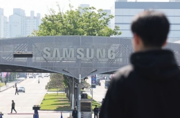
On the 21st, Samsung Electronics announced plans to establish a foundry facility at its Pyeongtaek semiconductor plant. A foundry refers to a semiconductor contract manufacturing service that produces chips on behalf of fabless companies, which are design firms without their own semiconductor production facilities.
Earlier, in April last year, Samsung Electronics announced its Semiconductor Vision 2030, which includes investing 133 trillion KRW and hiring 15,000 employees by 2030, aiming to become number one not only in memory semiconductors but also in system semiconductors (non-memory semiconductors). The recent investment plan for the Pyeongtaek foundry facility is part of the Semiconductor 2030 initiative.
Extreme Ultraviolet (EUV) equipment is considered the core of Samsung Electronics’ investment in the Pyeongtaek semiconductor foundry facility. As the Fourth Industrial Revolution accelerates, semiconductors such as CPUs, Application Processors (AP), image sensors, and modem chips are increasingly used in smartphones as well as in automobiles, advanced home appliances, and medical bio sectors to analyze and process data, all while becoming smaller in size. Meanwhile, fabless companies that do not have semiconductor production equipment but develop such ideas are also increasing.
EUV is used in the photolithography process, one of the dozens of steps in semiconductor manufacturing. The photolithography process involves projecting light through a mask containing circuit patterns onto a silicon wafer (semiconductor substrate) to draw the circuits, similar to developing a photograph. EUV has a wavelength less than one-fourteenth that of argon fluoride (ArF), which was previously used in photolithography, making it suitable for implementing finer semiconductor circuit patterns. It also reduces the need for multi-patterning processes that print complex circuits multiple times, enabling both high performance and productivity in semiconductors.
Even when using the same area of silicon wafer, EUV allows for producing more semiconductors. EUV is mainly used for manufacturing semiconductors with design nodes of 10 nanometers or less. Globally, only Samsung Electronics and Taiwan’s TSMC can mass-produce semiconductors at 7 nanometers or below. Samsung Electronics and TSMC are now competing to mass-produce 5-nanometer chips.

Besides improvements in semiconductor technology and productivity, EUV equipment also surprises with its price. EUV equipment is exclusively produced by the Dutch company ASML. Since ASML holds a monopoly on developing and selling this equipment, the price per unit is extremely high. Depending on the model, each unit costs approximately 150 billion to 200 billion KRW.
Hot Picks Today
![About 100 Trillion Won at Stake... "Samsung Strike Is an Unprecedented Opportunity" as Prices Surge 20% [Taiwan Chip Column]](https://cwcontent.asiae.co.kr/asiaresize/93/2026051416263163580_1778743590.jpg) About 100 Trillion Won at Stake... "Samsung Strike Is an Unprecedented Opportunity" as Prices Surge 20% [Taiwan Chip Column]
About 100 Trillion Won at Stake... "Samsung Strike Is an Unprecedented Opportunity" as Prices Surge 20% [Taiwan Chip Column]
- "Heading for 2 Million Won": The Company the Securities Industry Says Not to Doubt [Weekend Money]
- "Envious of Korean Daily Life"...Foreign Tourists Line Up in Central Myeongdong from Early Morning [Reportage]
- "Anyone Who Visited the Room Salon, Come Forward"… Gangnam Police Station Launches Full Staff Investigation After New Scandal
- Did Samsung and SK hynix Rise Too Much?... Foreign Assets Grow Despite Selling [Weekend Money]
As mentioned earlier, Samsung Electronics already holds the global number one market share in memory sectors such as DRAM and NAND flash. However, it has yet to claim the top spot in system semiconductors and foundry sectors. As of last year, Samsung Electronics held about 4% of the global system semiconductor market share, ranking around 5th to 6th place. According to market research firm TrendForce, in the first quarter of this year, Samsung Electronics ranked second in the foundry market share with 15.9%, following TSMC’s 54.1%. With Samsung Electronics’ continuous investments in semiconductor businesses, attention is focused on whether it can catch up to TSMC in the foundry sector by securing orders from global fabless companies such as Qualcomm.
© The Asia Business Daily(www.asiae.co.kr). All rights reserved.