Lee Jae-yong Attends Groundbreaking Ceremony of Samsung Semiconductor R&D Complex
Starting Full-Scale Management While Reviewing Next-Generation Semiconductor Development

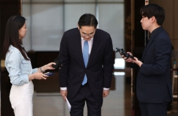
A photo of Vice Chairman Lee Jae-yong (second from the left) attending the groundbreaking ceremony at Samsung Electronics' Giheung Semiconductor R&D Complex on the 19th. From the left, Jeong Eun-seung, CTO of the DS Division; Vice Chairman Lee Jae-yong; Kyung Kye-hyun, Head of the DS Division; and Jin Gyo-young, President of Samsung Advanced Institute of Technology. Photo by Jeong Eun-seung
View original image[Asia Economy Reporter Park Sun-mi] Samsung Electronics Vice Chairman Lee Jae-yong chose the groundbreaking ceremony for the next-generation semiconductor research and development (R&D) complex as his first official external activity following the special pardon on August 15th, Liberation Day. This reflects his determination to make Samsung Electronics the world’s number one in system semiconductors by 2030 and to prioritize ‘technology’ as Samsung Electronics’ top priority.
On the 19th, Samsung Electronics held the groundbreaking ceremony for the semiconductor R&D complex at the Giheung Campus in Yongin, Gyeonggi Province. After being reinstated by the special pardon on Liberation Day, Vice Chairman Lee reviewed management issues at the Seocho headquarters and then personally attended the semiconductor R&D groundbreaking ceremony, marking his first official external activity since reinstatement. About 100 executives and employees attended the ceremony, including Vice Chairman Lee, Kyung Kye-hyun, head of the DS Division, Jung Eun-seung, CTO of the DS Division, Jin Gyo-young, head of Samsung Advanced Institute of Technology, Lee Jung-bae, head of the Memory Business Division, Choi Si-young, head of the Foundry Business Division, and Park Yong-in, head of the System LSI Business Division.
Immediately after the groundbreaking ceremony, Vice Chairman Lee visited the Hwaseong Campus for a meeting with employees and a DS Division presidents’ meeting. He listened to employees’ suggestions and exchanged various opinions on improving organizational culture to promote challenge and innovation. At the DS Division presidents’ meeting held at the Semiconductor Research Institute, they discussed ▲ major issues and risks surrounding the global semiconductor industry ▲ progress in next-generation semiconductor technology R&D ▲ and strategies to secure technological capabilities to achieve a super-gap.
The Giheung semiconductor R&D complex will be constructed on approximately 109,000㎡ (about 33,000 pyeong), and Samsung Electronics plans to invest about 20 trillion won by 2028 to develop the research complex, including a semiconductor R&D dedicated line scheduled to start operation in mid-2025. The R&D complex will serve as a core research base for semiconductor R&D fields such as ▲ memory ▲ fabless system semiconductors ▲ and foundry (semiconductor contract manufacturing).
This is the first time in eight years since the establishment of the Device Solution Research (DSR) at the Hwaseong site in Gyeonggi Province in 2014 that Samsung Electronics is building a new R&D center in Korea. Vice Chairman Lee’s choice of the semiconductor R&D groundbreaking ceremony as his first external activity is interpreted as a strong commitment to achieving world number one in the system semiconductor sector, including foundry, following memory semiconductors, as announced in the 2019 ‘System Semiconductor 2030 Vision.’
To become number one in system semiconductors, strengthening technological capabilities is essential. After his European trip in June, Vice Chairman Lee emphasized the importance of securing technology to reporters by saying, “First is technology, second is technology, third is technology.” He visited IMEC, Europe’s largest non-profit comprehensive semiconductor research institute established in Belgium by Belgium, France, and the Netherlands, to observe how next-generation and beyond-next-generation semiconductor technology research is progressing. It is known that he deeply felt the need for Samsung Electronics to take a more aggressive approach to securing advanced technology through active R&D.
Hot Picks Today
!["Heading for 2 Million Won": The Company the Securities Industry Says Not to Doubt [Weekend Money]](https://cwcontent.asiae.co.kr/asiaresize/93/2025050713592847164_1746593968.jpg) "Heading for 2 Million Won": The Company the Securities Industry Says Not to Doubt [Weekend Money]
"Heading for 2 Million Won": The Company the Securities Industry Says Not to Doubt [Weekend Money]
- Jay Y. Lee Bows His Head: "I Will Face the Harsh Storm"...Apologizes for Samsung Labor-Management Conflict
- "Drink Three Cups of Coffee and Stay Up All Night Before the Test"... Manual of Insurance Planner Who Collected 1 Billion Won in Payouts
- "Anyone Who Visited the Room Salon, Come Forward"… Gangnam Police Station Launches Full Staff Investigation After New Scandal
- "Wearing a Leather Jacket in 30-Degree Heat, Jensen Huang Enjoys Street Food as Beijing's 'Mukbang Star': 'It's Delicious'"
Vice Chairman Lee’s choice of Giheung as the destination for his first external activity also holds special regional significance. The Giheung Campus is symbolic as the place where the late Samsung Chairman Lee Byung-chul started the semiconductor business in the 1980s. Samsung, which currently holds the world number one position in memory semiconductors, began its semiconductor business in Giheung and has expanded domestically to Hwaseong and Pyeongtaek, and internationally to Xi’an, China, and Texas, USA. As Samsung’s ‘return to its original intention’ becomes crucial amid fierce semiconductor competition, Vice Chairman Lee’s selection of Giheung as the first site for on-site management after reinstatement is also a strong expression of his determination to create a ‘New Samsung.’
© The Asia Business Daily(www.asiae.co.kr). All rights reserved.