Foundry Struggled but Seeks Breakthrough with 2nm GAA Technology
Delayed Recovery in Mobile and PC Demand
Strengthening Competitiveness by Establishing 2nm Process
Challenges to Overcome Including Low Yield
On the 31st, Samsung Electronics announced its preliminary results for the third quarter of this year, expressing a strong commitment to establishing a 2nm (nanometer; 1nm is one billionth of a meter) process applying Gate-All-Around (GAA) technology to recover its foundry (semiconductor contract manufacturing) division, which is currently experiencing losses.

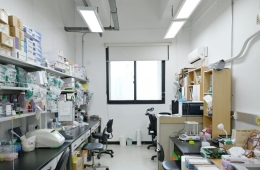
Samsung Electronics Seocho Building, Seocho-gu, Seoul. Photo by Jinhyung Kang aymsdream@
View original imageSamsung Electronics stated that its foundry "saw a decline in performance compared to the previous quarter due to weaker-than-expected recovery in demand for mobile and PC, as well as increased one-time costs," and added, "As the recovery in demand from key applications is delayed, we plan to focus on securing customers through expanding various applications and ensuring mass production capability of 2nm GAA."
During the briefing following the earnings announcement, the company also said, "Our 2nm GAA process is being developed as a platform technology optimized for mobile and HPC (high-performance computing) applications," and "We are targeting mass production of products in 2025 by improving process maturity and expanding the IP portfolio." It added, "Currently, major customers are evaluating performance, power, and area with our 2nm GAA PDK and design infrastructure, keeping customer productization in mind," and "For certain customers, key IPs and silicon characteristics used in products are being evaluated through MPW (multi-project wafer, a method of testing multiple designs on a single wafer simultaneously)."
Samsung Electronics was the first in the world to introduce the next-generation transistor structure, GAA technology, in its 3nm process in July 2022, but results fell short of expectations due to yield issues. Consequently, the company recently chose a strategy to apply GAA technology to the 2nm process to strengthen its foundry competitiveness. This announcement is interpreted as a public declaration of this direction and a focus on achieving a technological breakthrough in the 2nm process.
Samsung Electronics plans to secure new customers by developing a ‘Buffer Die’ solution for High Bandwidth Memory (HBM) in collaboration with its memory division. The buffer die is a device that efficiently manages data transmission at the bottom of HBM chips, which helps increase data transfer speeds and reduce power consumption, attracting industry attention.
However, Samsung Electronics stated that investment scale is expected to be reduced considering market conditions and investment efficiency. Song Tae-jung, Executive Vice President of Samsung Electronics’ Foundry Business Division, said at the earnings briefing, "We are prioritizing line conversion and managing foundry investments considering market conditions and investment efficiency," adding, "This year’s CAPEX (capital expenditure) is expected to decrease, and we plan to proceed cautiously and efficiently with profitability in mind." Regarding the foundry market situation, he explained, "Despite increased demand for AI and HPC in the third quarter, demand recovery in mobile and PC applications fell short of expectations," and "In the fourth quarter, customer demand is expected to remain weak due to delayed market rebounds in key applications."
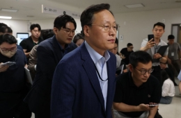
Samsung Electronics’ foundry is expected to face losses in the trillions of won this year as well, making a turning point necessary. Customer orders remain low, and low yields are also pointed out as challenges to overcome. Globally, its market share in the second quarter of this year was 11.5%, showing a 50.8 percentage point gap from the leader TSMC (Taiwan, 62.3%). As conditions have worsened, there has been a growing atmosphere outside the company recommending Samsung Electronics to spin off or dispose of its foundry business. However, Chairman Lee Jae-yong drew a clear line on the foundry spin-off rumors, saying, "We are not considering it," and emphasized, "We crave growth." This is interpreted as a firm policy to continue pushing forward with the foundry business.
Hot Picks Today
 "Stocks Are Not Taxed, but Annual Crypto Gains Over 2.5 Million Won to Be Taxed Next Year... Investors Push Back"
- [Breaking] Samsung Labor-Management 'Performance Bonus Negotiations' Fail in Third Mediation... Union Says "General Strike to Proceed as Planned Tomorrow"
- "Not Jealous of Winning the Lottery"... Entire Village Stunned as 200 Million Won Jackpot of Wild Ginseng Cluster Discovered at Jirisan
- Bull Market End Signal? Securities Firm Warns: "Sell SK hynix 'At This Moment'"
- "Even With a 90 Million Won Salary and Bonuses, It Doesn’t Feel Like Much"... A Latecomer Rookie Who Beat 70 to 1 Odds [Scientists Are Disappearing] ③
In this context, the regular personnel reshuffle, expected early next month, is also attracting attention. Samsung Electronics plans to demonstrate its determination to overcome the management crisis through personnel changes, with the foundry division being the top candidate for personnel renewal. The fate of the foundry plant under construction in Taylor, Texas, USA, also appears important. Industry experts continue to argue that for Samsung Electronics to receive many orders from global tech companies in the US in the future, the completion of the Taylor plant must be expedited. Samsung Electronics has, depending on company circumstances, withdrawn many dispatched personnel related to the Taylor plant and postponed its completion from the end of 2024 to 2026.
© The Asia Business Daily(www.asiae.co.kr). All rights reserved.