SK Hynix's Kwak No-jeong Meets Korea University Future Talent... "Leading the Future with Signature Memory"
Special Lecture on Memory Semiconductor Vision Held
"We will create SK Hynix's own 'Signature Memory' to satisfy the increasingly diverse demands of each customer. Since people are the ones who will create differentiated technology from the past, nurturing talent will be our top priority."
On the 2nd, SK Hynix President Kwak No-jeong said this during a special lecture held at Korea University Seoul Campus in Seongbuk-gu, Seoul. This lecture was held to secure future talent, and following a lecture last month at the Korea Advanced Institute of Science and Technology (KAIST), President Kwak visited his alma mater this time to share SK Hynix's business vision under the theme of 'Vision of Memory Semiconductors and Talent Development.'
On that day, President Kwak pointed to Signature Memory as the direction for the memory semiconductor business. Signature Memory refers to customer-customized memory specialized for specific performance. Memory has traditionally been used as a general-purpose product, but recent technological advances such as artificial intelligence (AI) have presented new challenges. SK Hynix plans to focus on AI and has succeeded in developing Signature Memory such as High Bandwidth Memory (HBM), aiming to strengthen competitiveness in related fields.

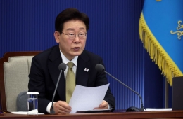
Kwak No-jeong, President of SK Hynix, is giving a special lecture on the theme of 'The Vision of Memory Semiconductors and Talent Development' on the 2nd at Korea University in Seongbuk-gu, Seoul. / Photo by SK Hynix
View original imagePresident Kwak said, "The core of the post-Von Neumann computing environment is likely to be memory in the future," adding, "just as SK Hynix has been preparing HBM for the past 10 years, we are putting a lot of effort into developing emerging memories based on Processing-In-Memory (PIM) and Compute Express Link (CXL), which could become the second and third HBM."
In the DRAM sector, they are simultaneously preparing process miniaturization and three-dimensional (3D) DRAM technology. They are also exploring a new DRAM cell structure that applies NAND flash stacking technology to DRAM. President Kwak explained, "There are still many issues to solve in terms of characteristics and cost, but if we overcome these, we can further advance DRAM technology."
Regarding NAND, where competition for stacking over 300 layers is underway, technological challenges are expected to increase after 500 layers. President Kwak explained that while advancing stacking technology, they are also developing wafer bonding technology necessary for lateral scaling. Additionally, they are considering technology to advance data storage methods from Triple-Level Cell (TLC) to Quad-Level Cell (QLC) and Penta-Level Cell (PLC) as alternatives.
As ESG realization has emerged as the top priority in the industry, SK Hynix is also focusing on creating an eco-friendly semiconductor production environment and introducing solution products with low power consumption. President Kwak explained that with the rapid increase of data centers, switching DRAM standards from Double Data Rate (DDR) 4 to DDR5 and replacing all Hard Disk Drives (HDD) with Solid State Drives (SSD) can significantly reduce greenhouse gas emissions.
Hot Picks Today
!["Not Everyone Can Afford This: Inside the World of the True Top 0.1% [Luxury World]"](https://cwcontent.asiae.co.kr/asiaresize/93/2026051507261063923_1778797570.png) "Not Everyone Can Afford This: Inside the World of the True Top 0.1% [Luxury World]"
"Not Everyone Can Afford This: Inside the World of the True Top 0.1% [Luxury World]"
- "We're Now Earning 10 Million Won a Month"... Semiconductor Boom Drives Performance Bonuses at Major Electronic Component Firms
- "I'm No Longer the Center?"... Even the World's Top Sniper Sidelined in the Era of Drones
- Handonghun: "I Will Win and Crush the Democratic Party's Tyranny"
- "Target Price Set at 970,000 Won"... Top Investors Already Watching, Only an 'Uptrend' Remains [Weekend Money]
He pointed out that securing talent is essential to realize these tasks. He explained that technology has been at the core of SK Hynix's ability to continue its business over the past 40 years despite various difficulties, and it is the talent that made this technology possible. President Kwak said, "We aim to create a global semiconductor hub with the three regions of Icheon, Cheongju, and Yongin as a triangular axis," and concluded the lecture by saying, "I look forward to the day when future talents like you will create a better world together with SK Hynix."
© The Asia Business Daily(www.asiae.co.kr). All rights reserved.