"Boosting Korean Production" Dutch ASM Invests 130 Billion Won to Expand Semiconductor Equipment
ASM Chooses Korea as Base for Business Expansion
Unveils Manufacturing and Research Innovation Center in Hwaseong, Gyeonggi
Expands PEALD Facilities for Domestic Research and Production
"This Investment Reflects Our Ambition to Grow Business in Korea"
ASM, a Dutch semiconductor equipment company, has chosen South Korea as a key hub to expand its business amid growing demand for advanced semiconductors. The company will invest $100 million (approximately 131.3 billion KRW) to launch a Manufacturing Research Innovation Center in Hwaseong, Gyeonggi Province, dedicated to plasma-enhanced atomic layer deposition (PEALD) equipment, which is researched and produced exclusively in South Korea.
"South Korea, the only research and production base for plasma-enhanced atomic layer deposition"
On the morning of the 23rd, ASM held a press conference at the Chosun Palace Seoul Gangnam. Ahead of the groundbreaking ceremony for the second Manufacturing Research Innovation Center in Hwaseong, Gyeonggi Province, scheduled for the 24th, the company revealed its investment background and future business plans in South Korea.
ASM previously opened an R&D and manufacturing center in Hwaseong, Gyeonggi Province, in 2019. This time, it will invest an additional $100 million to establish the second Manufacturing Research Innovation Center to expand its PEALD equipment business, which is exclusively researched and produced in South Korea.

Benjamin Ro, CEO of ASM, is speaking at a press conference held on the 23rd at Chosun Palace Seoul Gangnam. / Photo by ASM
View original imageThe new center will be specialized for PEALD. As an expansion project, the R&D area will more than double, and the manufacturing area will nearly triple compared to the existing center. The total area will be 31,000 square meters (㎡) and is scheduled for completion in 2025. The number of employees is expected to increase by about 200 over the next 3 to 5 years due to the expanded business space.
Benjamin Lo, ASM’s Chief Executive Officer (CEO), said, "PEALD equipment is used not only for DRAM and 3D NAND flash but also for logic (system) and other advanced semiconductors," adding, "We decided to invest because we expect demand in the PEALD field to increase for several years."
PEALD equipment is a type of atomic layer deposition (ALD) equipment used in semiconductor deposition processes. ALD equipment is used to form thin oxide films (thin films) by stacking atomic layers one by one on a wafer. Compared to other types of deposition equipment, it can reduce film thickness and achieve uniform thin films, but its limitation is low productivity.
PEALD equipment utilizes plasma (a state where gas is heated to an extremely high temperature and particles are divided into electrons, ions, etc.) properties to reduce the disadvantages and enhance the advantages of conventional ALD equipment. ASM acquired the domestic company GenieTech, which developed PEALD technology in 2005, and has since focused its related business in South Korea.
By 2030, semiconductor market expected to grow to $1 trillion... "Business opportunities in China still exist"
ASM is building competitiveness by collaborating with large domestic customers to contribute to technological advancement. The company explained that the market’s importance is significant because South Korea is home to semiconductor industry leaders such as Samsung Electronics and SK Hynix, who are dedicated to developing advanced semiconductor technologies. ASM’s business scale in South Korea ranks third after the United States and Singapore.
CEO Lo said, "This investment means more than just expanding facilities," adding, "It reflects our ambition to steadily grow ASM’s business here." He continued, "We will continue to support the development of advanced technologies in South Korea to lead global semiconductor innovation at a world-class level."

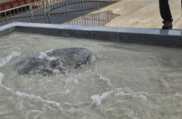
ASM 2nd Manufacturing Research Innovation Center bird's-eye view. Designed as an eco-friendly facility, it will be completed in 2025. / Photo by Kim Pyeonghwa
View original imageASM expects the semiconductor downturn that began in earnest last year to continue through this year but anticipates recovery starting next year. With increasing demand for semiconductors in areas such as 6th generation mobile communication (6G), electric vehicles, and generative artificial intelligence (AI), the global semiconductor market is expected to approach $1 trillion (approximately 1312 trillion KRW) by 2030.
Regarding the U.S. ban on exporting equipment used in advanced semiconductor production to China, which took effect in October last year, ASM maintains that business opportunities in China still exist. CEO Lo said, "The regulations target only the most advanced semiconductor equipment, not semiconductor-related equipment used in general products," adding, "We can continue our business in China."
Hot Picks Today
 If They Fail Next Year, Bonus Drops to 97 Million Won... A Closer Look at Samsung Electronics DS Division’s 600M vs 460M vs 160M Performance Bonuses
- Opening a Bank Account in Korea Is Too Difficult..."Over 150,000 Won in Notarization Fees Just for a Child's Account and Debit Card" [Foreigner K-Finance Status]②
- "While Others Rest, Nearly 3 Million May Work Substitute Public Holidays Without Extra Pay"
- "Better Than the Lottery": Reporting Collusion Could Earn Hundreds of Billions... KFTC Announces Administrative Notice to Abolish Whistleblower Reward Cap
- "Who Is Visiting Japan These Days?" The Once-Crowded Tourist Spots Empty Out... What's Happening?
ASM is one of the world’s top 10 semiconductor equipment companies headquartered in the Netherlands. It specializes in ALD and epitaxy equipment businesses and has bases in 15 countries, including South Korea. ASM entered the South Korean market in 1989 and expanded its business by establishing its subsidiary ASMK in 1995. The company currently employs about 460 people domestically.
© The Asia Business Daily(www.asiae.co.kr). All rights reserved.

!['WHO Declares International Public Health Emergency' Why the Untreatable 'Variant Ebola' Is More Deadly Than COVID-19 [Reading Science]](https://cwcontent.asiae.co.kr/asiaresize/307/2026052110164072055_1779326201.png)
!["Please Help Us": How Much Do Those Bowing 90 Degrees These Days Actually Earn? [Data Pick]](https://cwcontent.asiae.co.kr/asiaresize/307/2026052010120870131_1779239528.png)