Han also a memory powerhouse... Samsung and SK Hynix unveil next-generation memory technologies
'Flash Memory Summit 2022'
Samsung Ranks 1st for 20 Consecutive Years...Memory Solution 'Winning Move' in the Big Data Era
SK Hynix Successfully Develops the Highest Existing 238-Layer NAND

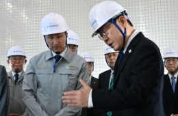
Samsung Electronics booth set up at the 'Flash Memory Summit 2022' event held at the Santa Clara Convention Center in the United States
View original image[Asia Economy Reporters Sunmi Park and Chaeseok Moon] Samsung Electronics and SK Hynix solidified South Korea's position as a 'memory semiconductor powerhouse' by unveiling a host of next-generation memory technologies and products at the world's largest flash memory industry conference, the 'Flash Memory Summit 2022.'
◆Samsung Tops for 20 Consecutive Years... Betting Big on Memory Solutions for the Big Data Era= On the 3rd, Samsung Electronics showcased numerous next-generation memory solutions essential for the big data era?including petabyte storage, memory-semantic SSDs, and telemetry?at the 'Flash Memory Summit 2022' held at the Santa Clara Convention Center in the United States.
Samsung Electronics first announced the capability to implement petabyte-class (1PB = 1 million GB) storage systems that enhance server system space utilization. As data demand surges beyond GB and TB into the 'PB era,' Samsung declared it can dramatically increase storage capacity, enabling vast amounts of data to be processed with minimal servers. This also offers the advantage of minimizing energy use through efficient server operation.
Samsung also unveiled a memory-semantic SSD based on the next-generation CXL interface. Memory-semantic SSDs are considered optimal solutions in fields that heavily utilize small-sized data, such as artificial intelligence (AI) and machine learning (ML). Compared to conventional SSDs, they can improve read speed and response time by up to 20 times in AI and ML applications.
Additionally, Samsung introduced telemetry technology that manages storage reliably. This technology detects abnormal signs in environments where SSDs are used in advance to prevent risks. As data explodes, technologies that manage each storage unit more stably within data centers are becoming increasingly important. Furthermore, Samsung announced plans to begin mass production this month of the industry's first UFS 4.0 memory developed in May. UFS 4.0 memory can be a core solution for flagship smartphones requiring rapid large-capacity processing, such as high-resolution content and high-capacity mobile games.
Samsung Electronics has held the number one position in the NAND market for 20 years with a 35.5% market share in the first quarter of this year. Notably, it has achieved outstanding results with 57.4% and 42.9% shares in the enterprise server and mobile markets, respectively, which demand high performance, large capacity, and low power consumption, far exceeding its overall market share. Choi Jin-hyuk, Vice President of the Memory Business Division's Solution Development Office at Samsung Electronics, said, "The explosive increase in data poses a significant challenge to the industry. Samsung Electronics will continue to lead various markets such as artificial intelligence, machine learning, and high-performance computing through innovative semiconductor solutions tailored to each area of data movement, storage, processing, and management."

◆SK Hynix Achieves Success in Developing the World's Tallest 238-Layer NAND= SK Hynix also announced at the summit that it succeeded in developing the world's tallest 238-layer NAND, demonstrating that Korean companies are the first to approach this 'dream technology.'
SK Hynix revealed its new 238-layer 512Gb (gigabit) TLC 4D NAND flash product and announced that samples have been released to customers. Full-scale mass production is planned for the first half of next year.
This achievement came just 1 year and 7 months after developing the 176-layer NAND in December 2020, marking success in next-generation technology development. The 238-layer NAND is especially significant as it is the tallest yet also the smallest product in the world. Productivity has increased by 34% compared to the previous 176-layer generation. Additionally, the data transfer speed of the 238-layer NAND is 2.4Gb per second, 50% faster than the previous generation. The 4D technology reduces cell area per unit compared to 3D while improving production efficiency. Energy consumption used by the chip when reading data is also reduced by 21%.
SK Hynix plans to first supply the 238-layer product for customer SSDs used in PC storage devices, then expand its application range to high-capacity SSDs for smartphones and servers. Next year, it also plans to introduce a 1Tb product with double the capacity of the current 512Gb.
Hot Picks Today
 "Samsung and Hynix Were Once for the Underachievers"... Hyundai Motor Employee's Lament
- Samsung Enterprise Labor Union: "We Respect Court’s Injunction Decision... General Strike to Proceed on the 21st as Planned"
- "Was This Delicious Treat Enjoyed Only by Koreans?"... The K-Dessert Captivating Japan
- U.S. Treasury Yields Surge Amid Iran War Uncertainty... Warning Signs for AI Tech Stock Rally
- "That? It's Already Stashed" Nightlife Scene Crosses the Line [ChwiYak Nation] ③
Choi Jung-dal, Vice President in charge of NAND development at SK Hynix, said, "With the 238-layer developed based on 4D NAND technology, we have secured global top-class competitiveness in terms of cost, performance, and quality."
© The Asia Business Daily(www.asiae.co.kr). All rights reserved.