Hanmi Semiconductor to Establish U.S. Subsidiary...Kwok Dongsin: "A Year of Quantum Leap in Performance"
Hanmi Semiconductor will establish its U.S. subsidiary, 'Hanmi USA,' by the end of this year, marking its full-scale entry into the local semiconductor market.
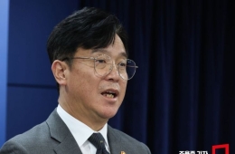
On May 15, Kwok Dongsin, Chairman of Hanmi Semiconductor, announced at the company’s Incheon headquarters, “Through our U.S. subsidiary, we plan to proactively and closely support the requirements of our clients on-site.” He added, “With the United States emerging as a global semiconductor production hub, we expect to secure substantial equipment orders in tandem with the operation of new factories, and we anticipate continued sales growth in the future.”

Dongshin Kwak, Chairman of Hanmi Semiconductor, is announcing plans to establish Hanmi USA Corporation at the company's headquarters in Incheon. Hanmi Semiconductor
View original imageHanmi Semiconductor plans to use its San Jose, California office as its integrated operational base, providing rapid technical support. This initiative aims to deploy skilled engineers locally and deliver proactive, close-knit technical assistance, aligned with the timeline for new factory operations by global semiconductor companies in the U.S.
Recently, as major Big Tech companies develop their own artificial intelligence (AI) semiconductors, there has been a growing trend of these firms directly reviewing and specifying the high-performance memory and the core equipment used in the manufacturing process. Consequently, demand for packaging equipment tailored to hyperscalers is expected to rise.
Chairman Kwok stated, “Driven by the continued increase in global demand for AI semiconductors, we expect a significant performance surge starting in the second quarter of this year, and anticipate a quantum leap in annual revenue from 2026 onward. As mass production of HBM4 ramps up this year, orders for TC Bonders are concentrated in the second quarter, and this momentum is expected to accelerate in the second half of the year.”
Currently, Hanmi Semiconductor holds the number one global market share in TC Bonders, which are essential for manufacturing high-bandwidth memory (HBM), the core of AI semiconductors. To further solidify its leadership in the next-generation HBM market, the company plans to launch a second-generation hybrid bonder equipment prototype within this year.
Hot Picks Today
 "Stocks Are Not Taxed, but Annual Crypto Gains Over 2.5 Million Won to Be Taxed Next Year... Investors Push Back"
- "Even With a 90 Million Won Salary and Bonuses, It Doesn’t Feel Like Much"... A Latecomer Rookie Who Beat 70 to 1 Odds [Scientists Are Disappearing] ③
- "Who Is Visiting Japan These Days?" The Once-Crowded Tourist Spots Empty Out... What's Happening?
- "Am I Really in the Top 30%?" and "Worried About My Girlfriend in the Bottom 70%"... Buzz Over High Oil Price Relief Fund
- "It Has Now Crossed Borders": No Vaccine or Treatment as Bundibugyo Ebola Variant Spreads [Reading Science]
Additionally, Hanmi Semiconductor is preparing to supply its '2.5D TC Bonder 40' and '2.5D TC Bonder 120'—packaging equipment for AI semiconductors—to foundries and outsourced semiconductor assembly and test (OSAT) companies this year. In the aerospace sector, which is a future growth driver, Hanmi Semiconductor began supplying the 'EMI Shield 2.0 X' series—launched earlier this year—to global aerospace companies, maintaining the number one market share in this field since its initial launch in 2016.
© The Asia Business Daily(www.asiae.co.kr). All rights reserved.