Lee Gyu-je, SK Hynix Vice President, "Diverse Next-Generation Packaging Needed to Maintain HBM Leadership"
Interview with Our Newsroom
Focus on Advanced MR-MUF and Hybrid Bonding
"Heat Generation Is a Challenge to Solve... Meeting Customer Demands"
Lee Kyu-je, Vice President in charge of PKG product development at SK Hynix, emphasized in an interview with the in-house newsroom on the 5th that in order for the company to maintain its leadership in the high-bandwidth memory (HBM) market, it is important to continuously respond to the increasing market demands and develop various next-generation packaging technologies.

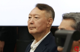
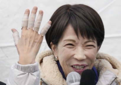
Lee Gyu-je, Vice President in charge of PKG Product Development at SK Hynix. Photo by SK Hynix Newsroom capture
View original imageIn the interview, Vice President Lee stated, "Next-generation packaging technologies such as hybrid bonding have recently attracted attention as a means of high-level chip stacking to improve performance and capacity while maintaining product thickness according to standard specifications." He added, "Although the heat dissipation issue caused by the reduced gap between the upper and lower chips remains a challenge to be solved, it is expected to be a solution that meets the increasingly diverse performance demands of customers." He further revealed, "SK Hynix plans to continuously advance the existing 'Advanced MR-MUF,' which has excellent heat dissipation performance, while securing new technologies."
SK Hynix is reviewing both the Advanced MR-MUF and hybrid bonding methods as packaging technologies for next-generation use. Advanced MR-MUF is a next-generation MR-MUF technology that applies chip control technology capable of stacking chips 40% thinner than existing chip thicknesses without warping, and improves heat dissipation characteristics through new protective materials. MR-MUF is a technology that bonds and molds a large number of chips, and Advanced MR-MUF is an enhanced version of this conventional method. Hybrid bonding is a technology that directly bonds chips without forming bumps between chips when stacking. This makes the overall chip thickness thinner, enabling high-level stacking. As the number of stacked chips bonded in recent HBM products has reached 16 layers or more, the necessity of this technology is being widely reviewed.
In particular, Vice President Lee cited the Advanced MR-MUF technology as the reason SK Hynix succeeded in developing the 4th generation 12-layer HBM3 and 5th generation HBM3E consecutively last year. He predicted that this technology "is also applied to the 12-layer HBM3E, which will be supplied to AI big tech companies from the second half of the year, and as its application range expands, it will help further solidify SK Hynix's top-tier HBM technology." He also recalled, "There was a rumor in the industry that MR-MUF was difficult to implement for high-level stacking. Because of this, we focused on communicating to customers that MR-MUF is the optimal technology for high-level stacking, and as a result, this became an opportunity to reaffirm customer trust."
Hot Picks Today
 Frozen Meals, Two Hours of Sleep... "I Wish I C...
- The Quoted 800,000 Won, the Bill Was 5 Million... Bereaved Families of 'No-Funer...
- "You Can Only Have This in Korea": Which National Museum Cafe Menu Is Captivatin...
- Tragedy in Luxury Apartment: Woman in Her 20s Found Dead, Suspect Identified
- "Never Hike Alone as a Woman" "Even Two Are at Risk"... Growing Fear of Crime on...
Vice President Lee emphasized, "The biggest driving force behind SK Hynix's ability to preoccupy the HBM market was providing products with quality and mass production competitiveness at the time customers wanted." He added, "The packaging development organization quickly identifies the needs of customers and stakeholders and reflects them in product characteristics. If we add the company's unique collaborative culture to these efforts, I believe it will exert strong power in any situation."
© The Asia Business Daily(www.asiae.co.kr). All rights reserved.