Samsung Electronics and Intel-Supported Applied Announce Patterning Solution for 2nm Implementation
Innovation in Semiconductor Patterning with Etching, Deposition, and Metrology
Major Foundries Currently Evaluating 2-Nanometer Implementation
Applied Materials, a U.S. semiconductor equipment company, has unveiled new etching and metrology systems ahead of the 2-nanometer (nm; 1 nm = one billionth of a meter) era. The company aims to achieve patterning innovation through systems that enhance production efficiency and yield amid increasing complexity in semiconductor process technology.

Applied Materials Korea held a media briefing on the 4th at its headquarters office in Bundang-gu, Seongnam City, to introduce new patterning solutions.
Patterning broadly refers to the overall process of creating circuits on wafers (silicon discs) in semiconductor manufacturing. It includes the lithography process that engraves circuit patterns on the wafer, the deposition process that stacks specific materials on the drawn patterns, and the etching process that removes the deposited materials in the shape of the patterns.
On this day, the company unveiled the 'Sym3 Y Magnum' etching system, which supports both deposition and etching, and the 'Producer XP Pioneer CVD' patterning film. These are designed to support extreme ultraviolet (EUV) processes introduced to implement fine circuits during patterning. Since next-generation EUV processes based on high numerical aperture (high NA) will be introduced to realize 2 nm products, these solutions are also intended to prepare for that.
Sym3 Y Magnum is a solution that deposits materials on the wafer and smooths the pattern drawn by EUV lithography equipment before the etching process, thereby improving yield while enhancing chip performance and power consumption. Pioneer is a hard mask material deposited on the wafer before drawing circuit patterns. It helps ensure that the patterns are drawn as intended.
Applied Materials explained that Sym3 Y Magnum has been adopted by major foundries and is being used in advanced processes. The company also stated that it is used in DRAM patterning work based on EUV processes. The Pioneer film is also being utilized by major memory manufacturers in the DRAM patterning process.
![Semiconductor Patterning Infographic / <br>[Photo by Applied Materials]](http://www.asiae.co.kr/news/img_view.htm?img=2024040415270829518_1712212028.jpg)
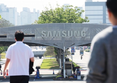
On the same day, Applied Materials also explained that the 'Centura Sculpta,' first introduced last year, is being used in Samsung Electronics' 4 nm foundry process and Intel's latest processes. Centura Sculpta is a patterning system that extends circuit patterns to reduce the EUV double patterning steps. It helps increase yield and reduce consumption costs. The company added a function to Centura Sculpta this year to eliminate bridge defects caused by narrow spacing between circuits.
Lee Gil-yong, head of technical marketing and strategic programs at Applied Materials Korea, said, "Using Centura Sculpta reduces investment and operating costs when designing fabs (factories). Currently, it is used in EUV lithography, but it can be used in conjunction with high NA when introduced." The company is currently conducting evaluations using Sculpta with major foundry companies to realize 2 nm technology.
The company also unveiled the advanced electron beam (eBeam) metrology system 'Acelta' on the same day. Its purpose is to reduce EUV patterning defects and help improve chip performance.
Hot Picks Today
 "Now Our Salaries Are 10 Million Won a Month" Record High... Semiconductor Boom Drives Performance Bonuses at Major Electronic Component Firms
- Experts Already Watching Closely..."Target Price Set at 970,000 Won" Only Upward Momentum Remains [Weekend Money]
- "Heading for 2 Million Won": The Company the Securities Industry Says Not to Doubt [Weekend Money]
- 'Still Hesitant? If You're Wondering Whether KOSPI Will Rise, This Is the Number You Must Watch [Weekend Money]'
- Is It Really Like an Illness? "I Can't Wait to Go Again"—Over 1 Million Visited in Q1, Now 'Busanbyeong' Takes Hold [K-Holic]
Park Kwang-sun, CEO of Applied Materials Korea, said, "As global manufacturers announce 2 nm and 1 nm process roadmaps, the importance of patterning to draw ultra-fine circuits on wafers is increasing," adding, "We will provide solutions to improve process efficiency beyond the nanometer scale into the angstrom (?; 1 ? = 0.1 nm) era."
© The Asia Business Daily(www.asiae.co.kr). All rights reserved.