Samsung's Focused 'Future Semiconductor Core Talent Team'... Recruiting Vice President from TSMC
Full Effort to Expand Newly Established AVP Business Team
Samsung Electronics has expanded its newly established AVP (Advanced Package) business team. Following the new graduate recruitment announcement earlier this year, the company is actively securing talent by hosting job-specific recruitment briefings. Semiconductor packaging is considered a key factor that will determine the future competitiveness of Samsung's foundry business as well as the memory sector.
Earlier in September, Samsung launched its second half open recruitment along with a recruitment briefing for the AVP business team. At that time, numerous posts related to the team's online briefing were shared across various university and job-related communities.
The AVP business team is a newly formed organization established this year. It is responsible not only for customer-tailored semiconductor packaging circuit design but also for product structure, material development, and simulation.
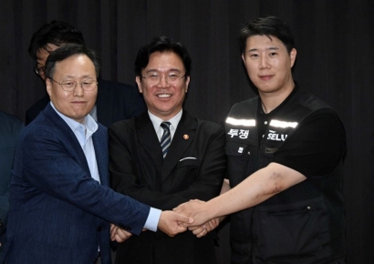
![Lee Jae-yong (second from the left), Chairman of Samsung Electronics, visited the Samsung Electronics Cheonan Campus last February to tour the packaging line and review business strategies. [Image source=Samsung Electronics]](http://www.asiae.co.kr/news/img_view.htm?img=2023121408492388255_1702511363.jpg)
Lee Jae-yong (second from the left), Chairman of Samsung Electronics, visited the Samsung Electronics Cheonan Campus last February to tour the packaging line and review business strategies. [Image source=Samsung Electronics]
View original imageIn the past, semiconductor companies focused on the miniaturization race to reduce nanometer (nm) scales, but now that the limits of fine processes have been reached, packaging technology is gaining attention.
Packaging is useful for extending semiconductor dies to create logic chips with more powerful performance. High Bandwidth Memory (HBM), adopted as a memory device for artificial intelligence (AI) semiconductors, is also a product that combines cutting-edge packaging technology with DRAM. Securing advanced packaging personnel has thus become a core element of future semiconductor competitiveness.
Samsung formed the AVP task force (TF) in June last year and launched the business team this year. Lin Jun-cheng, who worked at Taiwan's TSMC from 1999 to 2017, was also recruited as a vice president.
Hot Picks Today
 If They Fail Next Year, Bonus Drops to 97 Million Won... A Closer Look at Samsung Electronics DS Division’s 600M vs 460M vs 160M Performance Bonuses
- Opening a Bank Account in Korea Is Too Difficult..."Over 150,000 Won in Notarization Fees Just for a Child's Account and Debit Card" [Foreigner K-Finance Status]②
- Less Than a Year Later... Eunma Apartment Reconstruction Payments Surge by 300 Million Won
- "Manhole Cover Blasts Open in 12 Seconds... The Reason Behind the 'Gangnam Flood Disaster' [Report]"
- "Who Is Visiting Japan These Days?" The Once-Crowded Tourist Spots Empty Out... What's Happening?
In packaging technology, Korea is a latecomer compared to other semiconductor powerhouses. According to market research firm Yole D?veloppement, Taiwan dominates the semiconductor backend process market with a 52% share, exceeding half of the market. China ranks second with 21%, the United States is third with 15%, and Korea, ranked fourth, holds only 6%. This means that Korea has a relatively small pool of packaging personnel.
© The Asia Business Daily(www.asiae.co.kr). All rights reserved.
!['WHO Declares International Public Health Emergency' Why the Untreatable 'Variant Ebola' Is More Deadly Than COVID-19 [Reading Science]](https://cwcontent.asiae.co.kr/asiaresize/307/2026052110164072055_1779326201.png)
!["Please Help Us": How Much Do Those Bowing 90 Degrees These Days Actually Earn? [Data Pick]](https://cwcontent.asiae.co.kr/asiaresize/307/2026052010120870131_1779239528.png)