Samsung Joins Global Chip Packaging Standardization, Collaborates with Intel, TSMC, and Others
Pursuing Integration Efficiency Through 'UCIe' Chip Packaging Standard

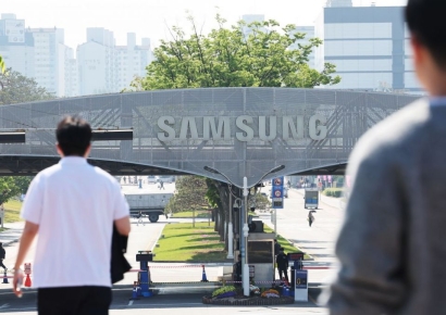
[Asia Economy Reporter Sunmi Park] Samsung Electronics is collaborating with global semiconductor companies such as Intel and TSMC to establish chip packaging standards.
According to industry sources on the 4th, Samsung Electronics has decided to cooperate with U.S.-based Intel and Taiwan's TSMC to develop next-generation chip packaging industry standards. They plan to form a consortium for collaboration related to chip packaging and stacking technologies, which are essential in the final stage of semiconductor processing. The consortium will also include global fabless semiconductor companies such as AMD, Qualcomm, and ARM, as well as technology companies like Google Cloud, Meta, and Microsoft.
The newly formed consortium aims to create a unified chip packaging standard called 'UCIe' to foster a new ecosystem and promote collaboration among companies in the chip packaging and stacking sectors.
This unprecedented cooperation among the world's leading semiconductor companies and technology firms clearly demonstrates how important chip packaging and stacking technologies have become in the semiconductor industry. Chip packaging technology, which belongs to the post-processing stage, was previously considered less critical and technically less challenging compared to front-end processes, as its difficulty and contribution to performance improvement were relatively lower. Until now, semiconductor development has focused mainly on integrating more transistors within a limited chip area to enhance performance.
However, recently, semiconductor companies including Samsung have been putting more effort into post-processing technologies to produce chips with stronger performance. This is because significant semiconductor performance improvements have become possible through post-processing as well.
Since the shorter the electron travel distance between transistors, the faster the semiconductor speed, foundry companies are focusing on narrowing the space between transistors. It has become important to efficiently package and stack small chips with various functions.
Samsung Electronics naturally welcomes this kind of industry collaboration. A Samsung official said, "If chip packaging standards are established through industry cooperation, it will open the way to more efficiently combine different types of chips, enabling the creation of more powerful chip systems."
This movement also aligns with the global trend where governments aiming to expand the semiconductor industry encourage cooperation among semiconductor companies to compensate for weaknesses in semiconductor competitiveness.
For example, the United States, which leads the global semiconductor market by leveraging strengths in semiconductor design and equipment, is attracting foundry fabs such as TSMC and Samsung Electronics through massive government support to compensate for its production sector, which is considered a weakness.
Hot Picks Today
 "Now Our Salaries Are 10 Million Won a Month" Record High... Semiconductor Boom Drives Performance Bonuses at Major Electronic Component Firms
- Wallets Open Wide on Big News...300 Trillion Won Heads to the U.S., "Tax Breaks" Fail to Keep Funds at Home
- "Hope You Enjoy the 'Welfare' for Bereavement of Children"... Ridicule of Strike Non-Participants Intensifies Union Conflict at Samsung Electronics
- "Heading for 2 Million Won": The Company the Securities Industry Says Not to Doubt [Weekend Money]
- Experts Already Watching Closely..."Target Price Set at 970,000 Won" Only Upward Momentum Remains [Weekend Money]
Japan, which has a weak production sector, and Taiwan, which is weak in equipment and materials, have also started government-level cooperation to complement each other's weaknesses. Researchers Choi Doyeon, Ko Youngmin, and Namgung Hyun from Shinhan Investment Corp. stated, "Although Korea has strengths in memory semiconductor production centered on Samsung Electronics and SK Hynix, there is a strong concentration in production, and weaknesses exist in non-memory fields as well as in design, equipment, materials/components, and post-processing sectors. It is necessary to find strategic cooperation partners to compensate for these weaknesses."
© The Asia Business Daily(www.asiae.co.kr). All rights reserved.