Successful Localization of New Materials Minimizing Contamination Particles in Semiconductor Manufacturing Equipment
Dr. Youngjo Park's Team at Korea Institute of Materials Science Develops 'Inflammasome Ceramic New Material' for the First Time in Korea

[Asia Economy Reporter Kim Bong-su] Domestic researchers have succeeded for the first time in Korea in developing a manufacturing technology for plasma-resistant nano-structured composite ceramics that can solve the particle issue, a major obstacle to semiconductor linewidth miniaturization.
The Korea Institute of Materials Science (KIMS) announced on the 3rd that Dr. Park Young-jo's research team at the Engineering Ceramics Laboratory, through joint research with private companies, has developed a new plasma-resistant ceramic material expected to reduce contamination particles inside semiconductor manufacturing equipment for the first time in Korea.
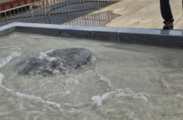
In semiconductor manufacturing, an etching process using plasma is generally performed. At this time, not only the silicon wafer but also the internal components of the equipment are exposed to plasma irradiation, generating contamination particles that are a major cause of chip defects. As semiconductor linewidths become finer, high-power plasma etching is required, making the development of new plasma-resistant materials to minimize contamination particle generation increasingly urgent.
When irradiating plasma for material etching, two variables to prevent contamination particles are maintaining a "low etching rate" and "small surface roughness." The research team applied the inorganic pore theory density densification sintering technology used in the development of transparent ceramics to yttria-magnesia (Y2O3·MgO) composite ceramics, achieving fully dense sintering without residual pores to minimize the etching rate. By combining plasma-resistant yttria (Y2O3) and magnesia (MgO) and minimizing grain growth during the sintering process, they achieved a fine structure at the 300-nanometer (nm) level, confirming the realization of the lowest surface roughness.
Among advanced process equipment in semiconductor manufacturing lines, a high proportion still depends on overseas sources. The research team explained that developing world-class plasma-resistant materials with domestic technology and applying these materials to process equipment upgrades is highly significant in securing a technological advantage in the global competition for linewidth miniaturization.
Hot Picks Today
 If They Fail Next Year, Bonus Drops to 97 Million Won... A Closer Look at Samsung Electronics DS Division’s 600M vs 460M vs 160M Performance Bonuses
- Opening a Bank Account in Korea Is Too Difficult..."Over 150,000 Won in Notarization Fees Just for a Child's Account and Debit Card" [Foreigner K-Finance Status]②
- Seoul Home Prices Surge as Listings from Multiple Homeowners Dwindle... Largest Rise in 16 Weeks
- Lived as Family for Over 30 Years... Daughter-in-Law Cast Aside After Husband's Death
- "Who Is Visiting Japan These Days?" The Once-Crowded Tourist Spots Empty Out... What's Happening?
The results of this research were published on the 13th of last month in the international academic journal Scientific Reports.
------------------------------------------------------------
© The Asia Business Daily(www.asiae.co.kr). All rights reserved.