"Quantum Dot Laser 'Mass Production' Technology Developed with Production Cost Reduced to 1/6"
A technology capable of mass-producing quantum dot lasers domestically has been developed. Quantum dot lasers are mainly used in data centers and quantum communication. With the possibility of mass production, the production cost is expected to be drastically reduced to about one-sixth of the existing level.
The Electronics and Telecommunications Research Institute (ETRI) announced on the 8th that its Optical Communication Components Research Lab at the headquarters has succeeded in developing indium arsenide/gallium arsenide (InAs/GaAs) quantum dot laser diodes usable in the 1.3㎛ wavelength band for optical communication on gallium arsenide (GaAs) substrates using metal-organic chemical vapor deposition (MOCVD) equipment.

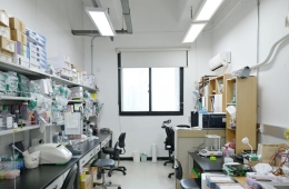
ETRI researchers are measuring the fabricated quantum dot laser diodes. Photo by ETRI
View original imagePreviously, quantum dot laser diodes were manufactured using molecular beam epitaxy (MBE) equipment. This equipment has a slow deposition rate, resulting in low production efficiency, making mass production difficult.
In contrast, the quantum dot manufacturing technology developed by the ETRI research team has the advantages of high quantum dot density and very uniformity. Above all, it can utilize large-area substrates with high defect density, enabling relatively easy reduction of process time and material costs.
For example, existing communication devices use expensive 2-inch indium phosphide (InP) substrates, resulting in very high manufacturing costs. However, the technology developed by the research team uses gallium arsenide (GaAs) substrates up to 6 inches in size, which cost less than one-third of indium phosphide substrates, and is expected to reduce the manufacturing cost of communication semiconductor lasers to less than one-sixth.
Additionally, the developed quantum dot semiconductor laser can operate continuously up to 75 degrees Celsius, which the research team emphasized is the world's highest level result achieved by metal-organic chemical vapor deposition.
The research team plans to enhance the research outcomes and increase reliability through verification, then transfer the technology to domestic optical communication companies. The companies receiving the technology will be supported with core technologies and infrastructure by the ETRI communication semiconductor foundry, which is expected to shorten the commercialization period of products.
The research results are expected to play a driving role in significantly reducing development time and production costs, increasing product price competitiveness, boosting overseas market share, and promoting the growth of the domestic optical communication components industry.
Hot Picks Today
 "Stocks Are Not Taxed, but Annual Crypto Gains Over 2.5 Million Won to Be Taxed Next Year... Investors Push Back"
- "Not Jealous of Winning the Lottery"... Entire Village Stunned as 200 Million Won Jackpot of Wild Ginseng Cluster Discovered at Jirisan
- Bull Market End Signal? Securities Firm Warns: "Sell SK hynix 'At This Moment'"
- "Greater Impact on Women Than Men"... The 'Diet Trap' That Causes Sleepless Nights and Suffering
- "Even With a 90 Million Won Salary and Bonuses, It Doesn’t Feel Like Much"... A Latecomer Rookie Who Beat 70 to 1 Odds [Scientists Are Disappearing] ③
Dr. Kim Hoseong of the ETRI Optical Communication Components Research Lab stated, “This research result is a case that simultaneously secures both commercial viability and originality,” and introduced it as “an important outcome that will be a turning point in changing the paradigm of the semiconductor laser industry for optical communication in the future.”
© The Asia Business Daily(www.asiae.co.kr). All rights reserved.