Minister Lee Jong-ho: "Semiconductor Advanced Packaging is a Core Technology"... 100 Billion Won Invested Over 5 Years
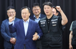
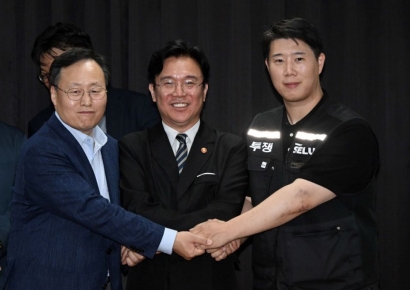
The Ministry of Science and ICT announced on the 30th that it visited LG Innotek to observe research sites related to substrates for advanced semiconductor packaging and held a roundtable meeting.
Presided over by Minister Jong-ho Lee, this roundtable was held to gather on-site opinions as the government plans to promote research and development (R&D) projects related to advanced semiconductor packaging next year. Industry, academia, and research experts participated, including Moon Hyuk-soo, CEO of LG Innotek; Kim Hyung-jun, Head of the Next-Generation Intelligent Semiconductor Business Group; Kang Sung-won, Vice President of the Electronics and Telecommunications Research Institute (ETRI); and Lee Ki-hyung, Vice President of Industry-Academic Cooperation at Hanyang University. During the meeting, they shared trends and the importance of advanced semiconductor packaging and discussed effective government R&D support policies and development plans. LG Innotek also presented the current status and plans for semiconductor substrate R&D, emphasizing the importance of securing core technologies.

Hwang Pan-sik, Director of Basic and Fundamental Research Policy at the Ministry of Science and ICT, stated, "Starting next year, we plan to promote R&D, workforce training, and international cooperation projects to secure core technologies related to advanced packaging," adding that more than 100 billion KRW will be invested over the next five years.
The new advanced packaging projects primarily aim to secure core technologies related to 3D stacking, high-efficiency and fine-pitch packaging, high-heat dissipation packaging structures, next-generation interposers, ultra-fine substrates, and substrate processes. A separate talent development project will also be promoted to train master's and doctoral-level specialists specialized in the advanced packaging field. This initiative is based on the 'Semiconductor Future Technology Roadmap' prepared jointly with related ministries in May of this year by the Ministry of Science and ICT.
Hot Picks Today
 If They Fail Next Year, Bonus Drops to 97 Million Won... A Closer Look at Samsung Electronics DS Division’s 600M vs 460M vs 160M Performance Bonuses
- Opening a Bank Account in Korea Is Too Difficult..."Over 150,000 Won in Notarization Fees Just for a Child's Account and Debit Card" [Foreigner K-Finance Status]②
- Foreign Media Take Note as Samsung Electronics Averts Strike Crisis: "Concerns Over AI Chip Supply Chain Eased"
- Room Prices Soar from 60,000 to 760,000 Won and Sudden Cancellations: "We Won't Even Buy Water in Busan" — BTS Fans Outraged
- "Who Is Visiting Japan These Days?" The Once-Crowded Tourist Spots Empty Out... What's Happening?
Minister Jong-ho Lee said, "Advanced packaging is a core technology that addresses the limits of semiconductor miniaturization, and competing countries have already recognized its importance and are actively investing at the national level," adding, "The Ministry of Science and ICT will strive to enhance semiconductor technological competitiveness through active investment in next-generation promising technologies."
© The Asia Business Daily(www.asiae.co.kr). All rights reserved.
!["Please Help Us": How Much Do Those Bowing 90 Degrees These Days Actually Earn? [Data Pick]](https://cwcontent.asiae.co.kr/asiaresize/307/2026052010120870131_1779239528.png)