[Report] Samsung Semiconductor's Ultra-Competitive Stage Pyeongtaek Campus... Overwhelmed by a Line Longer than Lotte Tower
Paper area 2.89 million ㎡... Equivalent to combined size of Giheung and Hwaseong campuses
Next-generation semiconductor frontline base... Basic construction of Line 4 underway

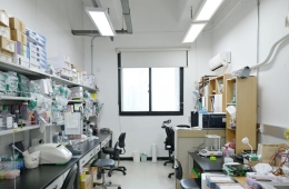
An employee wearing a white dustproof suit is inspecting the facility on Line 1 of the Pyeongtaek campus. / Source=Samsung Electronics
View original image[Asia Economy Reporter Kim Pyeonghwa] On the 7th, at Samsung Electronics' Pyeongtaek Campus semiconductor manufacturing facility, a glimpse into part of the process producing Samsung Electronics' DRAM revealed a thoroughly controlled environment that does not tolerate even fine dust, along with swiftly moving equipment, creating an unmissable spectacle. This experience made clear why the semiconductor industry is described as 'cutting-edge.'
The Pyeongtaek Campus, the heart of Samsung Electronics' semiconductor business and the world's largest semiconductor cluster, was unveiled to the media for the first time on this day. Established since 2015, the site covers an area of 2.89 million square meters (approximately 870,000 pyeong), equivalent to about 400 soccer fields. This is comparable to the combined size of Samsung Electronics' other semiconductor production bases, Giheung Campus (440,000 pyeong) and Hwaseong Campus (480,000 pyeong). A total of six production lines are planned to be established.
The third line, which began full-scale operation in July, is 700 meters long, making it the longest semiconductor building in the world. It is longer than the Lotte World Tower (555 meters) laid horizontally. This was the reason for the overwhelming impression during the facility tour. Classified as a national security facility, access by outsiders is strictly restricted. The third line, visited by President Joe Biden in May, is currently producing NAND flash memory semiconductors. Samsung Electronics aims to further solidify its dominance in the NAND flash market through this Pyeongtaek third line. About half of the third line will also be used for 14-nanometer DRAM and foundry processes below 5 nanometers.
Through the window tour set up at Line 1 (P1), some of the DRAM production processes could be observed beyond glass walls. A white wafer transfer device (OHT) rapidly moving across the ceiling caught attention. This device, responsible for transporting wafers to each process, was larger than a computer tower but operated at a swift speed of up to 5 meters per second. It was said that more than 1,500 OHTs are deployed per line.
Between the equipment, employees wearing cleanroom suits could also be seen. The cleanroom suits were not uniform in color but varied. For safety and security reasons, Samsung Electronics distinguishes colors: white for general employees, light sky blue for engineers, and dark blue for contractors. Due to the semiconductor process characteristics that do not allow even fine dust, cleanroom suits are essential. To prevent dust from the human body, even makeup was prohibited. The facility floor was absorbing dust to maintain factory cleanliness.

The Pyeongtaek Campus also houses a semiconductor museum. Here, visitors can learn about the process by which circular wafers undergo various steps to become multiple small semiconductors. When thinking of semiconductors, patterns on the surface come to mind, but over 300 processes are required to add patterns to a bare wafer. The explanation that producing a single semiconductor takes at least 90 days made this clear.
Hot Picks Today
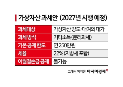 "Stocks Are Not Taxed, but Annual Crypto Gains Over 2.5 Million Won to Be Taxed Next Year... Investors Push Back"
- "Not Jealous of Winning the Lottery"... Entire Village Stunned as 200 Million Won Jackpot of Wild Ginseng Cluster Discovered at Jirisan
- "Rather Than Endure a 1.5 Million KRW Stipend, I'd Rather Earn 500 Million in the U.S." Top Talent from SNU and KAIST Are Leaving [Scientists Are Disappearing] ①
- "How Did an Employee Who Loved Samsung End Up Like This?"... Past Video of Samsung Electronics Union Chairman Resurfaces
- "Even With a 90 Million Won Salary and Bonuses, It Doesn’t Feel Like Much"... A Latecomer Rookie Who Beat 70 to 1 Odds [Scientists Are Disappearing] ③
Samsung Electronics is currently conducting foundational construction for Line 4 (P4) to establish the Pyeongtaek Campus as a next-generation semiconductor forward base. Since the Pyeongtaek Campus can accommodate a total of six lines, the facilities are expected to expand further in the future. Kyung Kye-hyun, CEO of Samsung Electronics DS, said, "It is growing into an advanced semiconductor complex production site where industry-leading 14-nanometer DRAM, ultra-high capacity V-NAND, and cutting-edge system semiconductors below 5 nanometers are produced," adding, "It will become the center of the domestic semiconductor ecosystem."
© The Asia Business Daily(www.asiae.co.kr). All rights reserved.