[Report] Visiting Samsung Semiconductor's Ultra-Leading Stage at Pyeongtaek Campus
Pyeongtaek Campus Larger Than Giheung and Hwaseong Campuses Combined
Examining DRAM Process Shows It Deserves the Title of 'Advanced' Industry
90 Days Required for One Semiconductor to Be Born
Samsung Prepares to Break Ground on Pyeongtaek Line 4... Establishing System for Timely Response to Future Semiconductor Demand

[Pyeongtaek=Asia Economy Reporter Kim Pyeonghwa] On the 7th, semiconductor manufacturing facilities at Samsung Electronics' Pyeongtaek Campus. The recently established line at the Pyeongtaek Campus boasted an overwhelming scale befitting its fame. Observing part of the process producing Samsung Electronics' DRAM, an unmissable scene unfolded with thoroughly maintained facilities that do not tolerate even fine dust and swiftly moving equipment. It made one truly feel why the semiconductor industry is described as 'cutting-edge.' Samsung Electronics plans to develop the Pyeongtaek Campus into an advanced semiconductor complex production site by adding more lines.
Pyeongtaek Campus Has Production Facilities 'Longer' Than Lotte World Tower
On this day, Samsung Electronics opened the Pyeongtaek Campus located in Godeok Industrial Complex, Pyeongtaek, Gyeonggi Province, to the media. The Pyeongtaek Campus is a semiconductor production base equipped with foundries producing memory semiconductors and system (non-memory) semiconductors. It is a representative site in the domestic semiconductor industry, visited by U.S. President Joe Biden during his visit to Korea in May.
It took about 1 hour and 30 minutes by car to get to the Pyeongtaek Campus from near City Hall Station in Jung-gu, Seoul, departing in the morning. As one left Seoul and approached the vicinity of the Pyeongtaek Campus, scenery typical of the outskirts of a city appeared. Buildings were sparse, and green backgrounds of trees and fields stood out. Upon reaching the Pyeongtaek Campus, a large gray-scale facility that could not be captured in a single glance spread out. It resembled The Hyundai Seoul in Yeouido, Seoul, at first sight. Many employees were actively moving in and out of the buildings.
Vehicle movement was essential within the Pyeongtaek Campus. With a total area of 2.89 million square meters (㎡), equivalent to 400 soccer fields, walking was impractical. It was said to be equivalent to the combined size of Samsung Electronics' other semiconductor production bases, Giheung Campus (440,000 pyeong) and Hwaseong Campus (480,000 pyeong), making it one of the largest semiconductor facilities. The campus had production facilities for a total of three lines, and the recently added Line 3 (P3) facility alone was 700 meters long, longer than the Lotte World Tower (555 meters) laid horizontally. This was the reason for the overwhelming impression while touring the facilities.

Employees of Samsung Electronics and its partner companies are walking along an internal road at the Pyeongtaek campus. / Source=Samsung Electronics
View original imageWafer Transfer Devices Busily Moving from the Ceiling... Dust-Proof Suit Colors Vary for Safety and Security
Through the window tour set up in Line 1 (P1), part of the process producing actual DRAM could be seen beyond the glass wall. Several white wafer transfer devices (OHT) moving rapidly around every corner of the facility from the ceiling immediately caught the eye. Although they appeared larger than a computer mainframe, their movements were not sluggish. Since they transport wafers to each process, they operated swiftly.
There are about 1,500 OHTs in P1 alone, operated by an automated system. These devices were introduced through Semes, a domestic semiconductor equipment company. Samsung Electronics said that the development of OHT simplified the process. Since OHT is an important piece of equipment in the process, it was also explained that the price of one unit reaches around 40 million KRW, comparable to the full-option price of a Hyundai Motor Grandeur model.
Through the glass wall, employees wearing dust-proof suits could also be seen moving between the equipment. A notable point was that the dust-proof suits were not uniform in color but varied. Samsung Electronics explained that for safety and security reasons, general employees wear white, engineers wear light sky blue, and partners wear dark blue suits. In fact, partner employees wore dark blue dust-proof suits with a cloth about the size of an A4 sheet attached to their chest displaying the partner company’s name.
Due to the semiconductor process characteristics that do not allow even fine dust, dust-proof suits are essential, and since dust also comes from the human body, even hair is thoroughly covered. Since makeup and rubbing eyes can generate about 25,000 dust particles instantly, makeup was prohibited along with wearing dust-proof suits. The facility floors had many small holes to absorb dust and maintain factory cleanliness.

An employee wearing workwear is walking at Samsung Electronics Pyeongtaek Campus P1. Rectangular-shaped OHTs are moving on the ceiling. Photo by Samsung Electronics
View original imageSamsung Conducts Foundation Work for Pyeongtaek Line 4... Towards an Advanced Semiconductor Complex Production Site
The Pyeongtaek Campus also featured a semiconductor museum where Samsung Electronics' semiconductor business and future vision could be explored. Here, visitors could learn about the process by which a circular wafer undergoes various steps to become multiple small semiconductors.
When thinking of semiconductor images, people often recall the patterns on the surface, but it was explained that over 300 processes are required to add patterns to a bare wafer. After this, post-processes including packaging and testing must be completed before the final semiconductor is born. It was understood that making one semiconductor takes at least 90 days, including eight major processes and post-processes.

3nm wafer signed by President Yoon Suk-yeol and U.S. President Joe Biden during their visit to the Pyeongtaek campus in May / Source=Samsung Electronics
View original imageSamsung Electronics has started additional line construction work to develop the Pyeongtaek Campus as a forward base for next-generation semiconductors. To respond promptly to future semiconductor demand, foundation work for Line 4 (P4) construction is underway. The specific construction start time and applicable products have not yet been decided. Since the Pyeongtaek Campus can accommodate a total of six lines, facilities are expected to expand further, including P4.
Hot Picks Today
!["Rather Than Endure a 1.5 Million KRW Stipend, I'd Rather Earn 500 Million in the U.S." Top Talent from SNU and KAIST Are Leaving [Scientists Are Disappearing] ①](https://cwcontent.asiae.co.kr/asiaresize/93/2026051414165763158_1778735817.jpg) "Rather Than Endure a 1.5 Million KRW Stipend, I'd Rather Earn 500 Million in the U.S." Top Talent from SNU and KAIST Are Leaving [Scientists Are Disappearing] ①
"Rather Than Endure a 1.5 Million KRW Stipend, I'd Rather Earn 500 Million in the U.S." Top Talent from SNU and KAIST Are Leaving [Scientists Are Disappearing] ①
- "If That's the Case, Why Not Just Buy Stocks?" ETFs in Name Only, Now 'Semiconductor-Heavy' and a Playground for Short-Term Traders
- Individual Investors Absorb Foreign Sell-Off... Concerns Over Becoming "Cannon Fodder" Emerge
- "It Will Be Quite Rare for People to Drive Themselves"... Musk's Optimism on Autonomous Driving
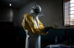
- "No Cure Available, Spread Accelerates... Already 105 Dead, American Infected"
Samsung Electronics CEO Kyeong Kye-hyun said, "The Pyeongtaek Campus is growing into an advanced semiconductor complex production site where the industry's most advanced 14nm DRAM, ultra-high capacity V-NAND, and advanced system semiconductors below 5nm are all produced. We will not only produce semiconductors but also build an eco-friendly workplace and engage in various win-win activities with local communities and partners, becoming the center of the domestic semiconductor ecosystem."
© The Asia Business Daily(www.asiae.co.kr). All rights reserved.
![Cheaper Than Mychew, but Nowhere to Be Found... Fears of a 'Pediatric Medical Crisis' as Drug Makers Halt Production [Why&Next]](https://cwcontent.asiae.co.kr/asiaresize/307/2026051910065268365_1779152813.jpg)