[Photo] Samsung Electronics Holds World’s First 3nm Semiconductor Mass Production Shipment Ceremony
![[Photo] Samsung Electronics Holds World’s First 3nm Semiconductor Mass Production Shipment Ceremony](http://www.asiae.co.kr/news/img_view.htm?img=2022072510471162243_1658713631.jpg)
On the morning of the 25th, at Samsung Electronics Hwaseong Campus in Hwaseong-si, Gyeonggi-do, officials are moving wafers onto a truck during the 'World's First GAA-based 3nm Mass Production Shipment Ceremony.' / Hwaseong = Reporter Kim Hyun-min kimhyun81@
Hot Picks Today
 "You Might Regret Not Buying Now"... Overseas Retail Investors Stirred by News of Record-Breaking Monster Stocks' IPOs
- "Not Jealous of Winning the Lottery"... Entire Village Stunned as 200 Million Won Jackpot of Wild Ginseng Cluster Discovered at Jirisan
- Mistaken for the Flu, Left Untreated... Death Toll Surges as WHO Declares Emergency (Comprehensive)
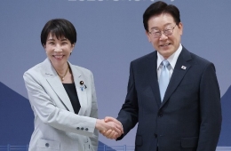
- Takaichi Says, "I Was Debating Drinking Due to Parliament Schedule"... President Lee Jokes, "Should I Make a Call?"
- "How Did an Employee Who Loved Samsung End Up Like This?"... Past Video of Samsung Electronics Union Chairman Resurfaces
This content was produced with the assistance of AI translation services.
© The Asia Business Daily(www.asiae.co.kr). All rights reserved.