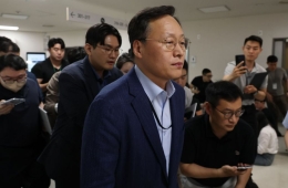
[Photo] Researchers Shipping Samsung Electronics 3nm Process Mass Production Products
![[Photo] Researchers Shipping Samsung Electronics 3nm Process Mass Production Products](http://www.asiae.co.kr/news/img_view.htm?img=2022072510472162244_1658713642.jpg)
On the morning of the 25th, at Samsung Electronics Hwaseong Campus in Hwaseong-si, Gyeonggi-do, officials are moving wafers onto a truck during the 'World's First GAA-based 3nm Mass Production Shipment Ceremony.' / Hwaseong = Reporter Kim Hyun-min kimhyun81@
Hot Picks Today
 "Stocks Are Not Taxed, but Annual Crypto Gains Over 2.5 Million Won to Be Taxed Next Year... Investors Push Back"
- "Don't Throw Away Coffee Grounds" Transformed into 'High-Grade Fuel' in Just 90 Seconds [Reading Science]
- Despite Warnings of "Do Not Enter, You May Not Make It Out Alive"... Foreign Tourist Stranded After Unauthorized Climb on Jeju Sanbangsan
- Signed Without Viewing for 1.6 Billion Won... Jamsil and Seongbuk Jeonse Prices Jump 200 Million Won in a Month [Real Estate AtoZ]
- "Even With a 90 Million Won Salary and Bonuses, It Doesn’t Feel Like Much"... A Latecomer Rookie Who Beat 70 to 1 Odds [Scientists Are Disappearing] ③
This content was produced with the assistance of AI translation services.
© The Asia Business Daily(www.asiae.co.kr). All rights reserved.