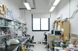
K-Semiconductor 'Weakness' Strengthened in Back-End Process [New Economic Security Landscape]
⑥China's Pause Creates Opportunity... Samsung, SK, Doosan, and OCI Expand Back-End Processing
![K-Semiconductor 'Weakness' Strengthened in Back-End Process [New Economic Security Landscape]](http://www.asiae.co.kr/news/img_view.htm?img=2022052310072876477_1653268048.jpg)
[Asia Economy Reporter Park Sun-mi] Korean companies, which have been relatively weak in the semiconductor back-end process (packaging and testing) sector, have begun strengthening their back-end process businesses. The plan is to expand investment in the back-end process business, located at the very end of the semiconductor value chain, to enhance the competitiveness of the semiconductor industry's value chain.
In particular, China, which has been showing aggressive moves in the system semiconductor sector including fabless (design), foundry (contract manufacturing), and back-end processes, is actively taking advantage of the situation where it is staggering due to repeated regional lockdowns and factory shutdowns.
According to the industry on the 5th, Samsung Electronics has organized an 'Advanced Packaging Commercialization' task force (TF) team under the DS Division head (President) Kyung Kye-hyun since last month to explore ways to utilize advanced packaging technology. Samsung Electronics has continuously strengthened its packaging technology, which belongs to the back-end process, by developing the industry's first '12-layer 3D-TSV (3D Through Silicon Via)' technology in 2019, the 'X-Cube' technology vertically stacking logic chips and SRAM in 2020, and last year the 'I-Cube4' technology that integrates a logic chip and four HBM (High Bandwidth Memory) chips into a single package.
An industry insider said, "Advanced packaging technology, which connects different types of semiconductors vertically or horizontally with wiring as thin as 1/60th of a hair to create a single system semiconductor, has become a core competitive edge," adding, "Samsung Electronics is also strengthening next-generation packaging solutions such as 2.5D and 3D to meet the characteristics required in various applications including artificial intelligence (AI), edge computing, high-performance computing (HPC), 5G, and autonomous driving."
SK Hynix has also recognized the importance of next-generation packaging technology and is focusing on securing competitiveness in TSV technology. It developed the third-generation version of HBM, HBM2E, applying TSV technology in 2019, and succeeded in mass production within 10 months, securing the number one market share in the HBM market. In October last year, it developed the world's first 'HBM3,' the highest specification DRAM currently available, and since last month, after completing all customer certifications, it has started mass production and supply of HBM3 to customers worldwide.
The fact that Korea's leading semiconductor companies Samsung and SK are undertaking supplementary work to develop back-end process technology is to produce chips with even stronger performance. As it becomes more important how to most efficiently package and stack small chips with various functions, significant semiconductor performance improvements have become possible solely through back-end process enhancements.
Recently, companies that were not previously involved in the semiconductor business have also entered the semiconductor back-end process field, creating an atmosphere of supplementing K-semiconductor weaknesses. Doosan announced plans to invest about 1 trillion won in the semiconductor business over the next five years and acquired Doosan Testna, specializing in testing conducted after semiconductor design and manufacturing, in April. The goal is to enter the global 'Top 5' in the semiconductor testing field centered on Doosan Testna. Additionally, it has recently started reviewing the acquisition of another semiconductor back-end process company, 'EngineOn.'
OCI also acquired a company engaged in the semiconductor back-end process business through its affiliates last year and is recently expanding into the automotive semiconductor testing market.
Korea's late entry into the semiconductor back-end process sector, dominated by Taiwan (52%), China (21%), and the United States (15%), is largely due to the very steep market growth potential.
According to market research firm TrendForce, the semiconductor packaging and testing market revenue is expected to reach $101.185 billion this year, growing 23.19% compared to the previous year. Last year's market size was $82.139 billion, growing 25.83%. China, leading the semiconductor back-end process industry, showed the fastest growth with a 31.7% increase in packaging and testing production last year, but recent factory shutdowns due to the 'Zero COVID' policy have put a brake on growth.
Hot Picks Today
 "Stocks Are Not Taxed, but Annual Crypto Gains Over 2.5 Million Won to Be Taxed Next Year... Investors Push Back"
- "Not Jealous of Winning the Lottery"... Entire Village Stunned as 200 Million Won Jackpot of Wild Ginseng Cluster Discovered at Jirisan
- One in 77 Koreans Exposed to Drugs... Enough Money for 6,600 Luxury Gangnam Apartments Circulates in Drug Market [ChwiYakGukga] ⑩
- "Greater Impact on Women Than Men"... The 'Diet Trap' That Causes Sleepless Nights and Suffering
- "Even With a 90 Million Won Salary and Bonuses, It Doesn’t Feel Like Much"... A Latecomer Rookie Who Beat 70 to 1 Odds [Scientists Are Disappearing] ③
An industry official said, "As demand for high-performance, high-capacity, ultra-high-speed semiconductors surges, packaging technology that boosts product speed and testing technology that verifies performance have become important," adding, "Korea has been weak in the back-end process field, but it is now entering a period of change."
© The Asia Business Daily(www.asiae.co.kr). All rights reserved.