TSMC "Securing ASML's Next-Gen EUV Equipment in 2024... Mass Production Timing 'Uncertain'"
![[Image source=AP Yonhap News]](http://www.asiae.co.kr/news/img_view.htm?img=2022052011265574353_1653013615.jpg)
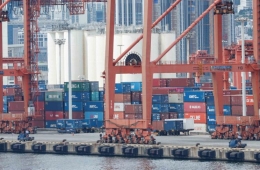
[Asia Economy Reporter Jeong Hyunjin] Taiwan's TSMC, the world's largest foundry (semiconductor contract manufacturing) company, announced that it will secure the next-generation extreme ultraviolet (EUV) lithography equipment 'High Numerical Aperture (NA) EUV' from Dutch semiconductor equipment maker ASML in 2024.
According to major foreign media on the 16th (local time), YJ Mi, Vice President of Research and Development (R&D) at TSMC, revealed this at the TSMC Technology Symposium held in Silicon Valley, USA. EUV lithography equipment is essential for implementing ultra-fine semiconductor processes and is exclusively produced worldwide by ASML.
'High NA EUV' is currently the most advanced next-generation EUV lithography equipment. Earlier this year, US company Intel announced that it had signed a contract to introduce this equipment ahead of ASML's two major customers, TSMC and Samsung Electronics, and plans to start product manufacturing using this equipment by 2025.
The Vice President did not disclose the timing for mass production of semiconductors using High NA EUV. Kevin Zhang, Senior Vice President of Business Development at TSMC, said that they would not be ready to deploy High NA EUV for mass production in 2024 and would mainly use it for mass production preparation research with partners.
Hot Picks Today
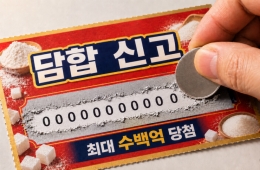
 At President Lee's Call to "Give Enough to Shock," Whistleblower Rewards Become a Real Lottery
- If They Fail Next Year, Bonus Drops to 97 Million Won... A Closer Look at Samsung Electronics DS Division’s 600M vs 460M vs 160M Performance Bonuses
- "While Others Rest, Nearly 3 Million May Work Substitute Public Holidays Without Extra Pay"
- Opening a Bank Account in Korea Is Too Difficult..."Over 150,000 Won in Notarization Fees Just for a Child's Account and Debit Card" [Foreigner K-Finance Status]②
- "Who Is Visiting Japan These Days?" The Once-Crowded Tourist Spots Empty Out... What's Happening?
At the symposium, TSMC explained its 2-nanometer (nm; 1 nanometer = one billionth of a meter) process technology aimed for mass production in 2025. TSMC plans to apply its 'nanosheet' transistor technology, which has been developed over 15 years and features a paper-thin and elongated shape, to the 2-nanometer process for the first time to improve semiconductor operating speed and power efficiency.
© The Asia Business Daily(www.asiae.co.kr). All rights reserved.