Intel pouring money into foundries... Companies betting their lives on 'ecosystem expansion' (Comprehensive)
Intel's 'Aggressive Moves' Announce $1 Billion Fund
Samsung Also Focuses on Ecosystem Building by Hosting SAFE Forum Annually

[Asia Economy Reporter Lee Hyeyoung] Global semiconductor companies, heralding a "foundry (semiconductor contract manufacturing) showdown," are putting their lives on building ecosystems. Intel, which declared its re-entry into the foundry business, has launched a large-scale fund to secure an ecosystem and is chasing TSMC and Samsung Electronics.
Samsung Electronics, which has been focusing on creating a semiconductor ecosystem, plans to accelerate innovation in foundry and system semiconductors this year by strengthening cooperation with its partners.
On the 7th (local time), Intel's independent foundry division IFS and Intel Capital announced the establishment of a $1 billion (approximately 1.2 trillion KRW) fund to build a foundry innovation ecosystem. The fund will prioritize investments in areas that can accelerate the launch of intellectual property, software tools, innovative semiconductor architectures, and advanced packaging technologies.
Intel is expected to form partnerships with several companies affiliated with the fund to support next-generation advanced packaging processes and share technologies with customers. It also announced strategic industrial changes such as developing modular products with an open chiplet platform and expanding the scope of the open instruction set architecture (ISA) 'RISC-V' for chip design.
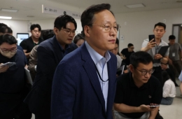
Pat Gelsinger, Intel CEO, said, "The semiconductor design ecosystem is crucial to the success of Intel's foundry division," adding, "Through the ecosystem fund and open chiplet platform, we will operate an ecosystem that can develop innovative technologies across chip architectures."
Intel also announced the launch of the foundry ecosystem called 'IFS Accelerator,' which aims to provide comprehensive support to smoothly carry out all semiconductor-related stages from design to execution and production.

Once the "absolute powerhouse" in semiconductors, Intel's status has declined as it struggled in its core central processing unit (CPU) field and lost ground in the technology speed race. Last year, it faced a crisis when it lost the title of "No. 1 semiconductor company" to Samsung Electronics.
As a countermeasure, Intel announced its re-entry into the foundry business with 'IDM 2.0,' deciding to invest a total of $40 billion by building foundry plants in Arizona and Ohio with $20 billion each. The U.S. government and Congress are also pushing a semiconductor support bill worth $52 billion, making massive funding visible.
Foundry companies see the importance of building and expanding foundry ecosystems growing as the "money war" intensifies. With technological advancement, the introduction of cutting-edge processes, and increasing design complexity, attracting as many fabless (design-specialized companies) as possible into the ecosystem becomes a decisive factor for business success from the foundry companies' perspective.
As major IT companies like Google, Apple, and Microsoft (MS) jump into developing their own semiconductors, the capabilities and technological competitiveness of foundries that produce these chips have become more important than ever. TSMC and Samsung, ranked first and second in global foundry market share, are engaging in a "nano war" (nm; 1 nanometer is one-billionth of a meter) with bold investments, while Intel, aiming to open the angstrom (0.1 nm) era, declared its intention to lead, all within this context.

TSMC, a pioneer in building foundry ecosystems, is also striving to secure the competitiveness of partner companies supporting customers' chip designs by establishing a VCA (Value Chain Aggregator).
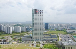
Samsung Electronics has also been building its foundry ecosystem with a long-term perspective. In 2018, Samsung unveiled the 'SAFE (Samsung Advanced Foundry Ecosystem)' program to build a foundry ecosystem and has held forums annually since 2019 to share technology trends and strengthen cooperation.
Through this, Samsung provides partners with opportunities to explain and discuss solutions in essential areas for semiconductor design and production, including EDA, IP, cloud, design, and packaging. At the forum held in November last year, under the theme 'Performance Platform 2.0,' they discussed ways to strengthen solutions necessary for chip implementation based on cutting-edge processes and expanded infrastructure with partners.
As a result, Samsung secured more than 80 EDA tools and technologies, including design infrastructure optimized for the 3nm GAA (Gate-All-Around) structure scheduled for mass production in the first half of this year, 2.5D and 3D package design solutions, and AI-based EDA.
Hot Picks Today
 "Stocks Are Not Taxed, but Annual Crypto Gains Over 2.5 Million Won to Be Taxed Next Year... Investors Push Back"
- "Don't Throw Away Coffee Grounds" Transformed into 'High-Grade Fuel' in Just 90 Seconds [Reading Science]
- [Breaking] President Lee: "Israel Violated All International Norms" in Abduction of Citizens in Gaza Strip
- "Groups of 5 or More Now Restricted"... Unrelenting Running Craze Leaves Citizens and Police Exhausted
- "Even With a 90 Million Won Salary and Bonuses, It Doesn’t Feel Like Much"... A Latecomer Rookie Who Beat 70 to 1 Odds [Scientists Are Disappearing] ③
Kim Yangpaeng, a senior researcher at the Korea Institute for Industrial Economics & Trade, said, "For foundry companies to secure customers, building an ecosystem is very important. Establishing a solid ecosystem that attracts as many design companies as possible and shares IP is an essential requirement to be chosen by global companies, and this directly relates to foundry survival and competitiveness."
© The Asia Business Daily(www.asiae.co.kr). All rights reserved.