Research Achievements on Next-Generation Semiconductor Materials Supported by Samsung Published in Leading International Journal
[Asia Economy Reporter Su-yeon Woo] Research on next-generation semiconductor materials by a domestic university research team supported by the Samsung Future Technology Development Program has been recognized and published in a world-renowned academic journal.
According to Samsung on the 25th, the research team led by Professors Junwoo Son and Siyoung Choi of the Department of Materials Science and Engineering at POSTECH developed next-generation semiconductor material technology to solve heat generation issues, and their achievements were published on the 18th of this month in the international academic journal Nature Communications.
The research team developed next-generation material technology to address the increasingly important heat issues caused by semiconductor miniaturization, and this technology was recognized as a material development achievement applicable to highly integrated semiconductors. The team was selected as a research project under the Samsung Future Technology Development Program in July 2017 and received support for three years, alongside support from the Basic Research Laboratory of the National Research Foundation of Korea.

POSTECH research team that succeeded in developing next-generation semiconductor materials supported by the Samsung Future Technology Development Program. (Back row from left) Professor Son Jun-woo, Professor Choi Si-young (Front row from left) Student Lee Dong-gyu, Dr. Park Yoon-kyu, Student Shim Hye-ji / Photo by Samsung Electronics
View original imageResearch Team Develops Alternative Material Technology... Solving Heat Generation Issues Due to Semiconductor Miniaturization
Technological innovation in the semiconductor field has progressed toward increasing the integration density of transistor circuits through miniaturization. As semiconductor integration increases, power consumption decreases and operating speed increases, but new problems such as malfunctions caused by heat generated during semiconductor operation are becoming more likely.
The solution involves lowering the driving voltage of transistors and developing new materials to replace conventional silicon or bonding silicon with new materials. Both academia and industry have devoted significant efforts to solving this problem.
A representative new material attracting attention is the 'phase transition oxide semiconductor,' which rapidly changes its phase from an insulator to a metal upon reaching a certain voltage. The research team focused on single-crystal vanadium oxide (a compound formed by bonding metallic vanadium and oxygen), a type of phase transition oxide semiconductor, which requires a lower voltage to conduct current compared to conventional silicon, thereby reducing heat generation. They developed technology to stack single-crystal vanadium oxide on silicon wafers.
However, since single-crystal vanadium oxide has a different crystal structure from silicon, direct stacking growth on the wafer could cause electrical defects. To address this, the research team first stacked titanium oxide, which has the same crystal structure, on the silicon wafer and then successfully grew vanadium oxide in a single-crystal state on top.
Professor Son said, "Through this research, the excellent properties of single-crystal phase transition oxides, which are attracting attention as next-generation materials, can now be applied to existing silicon semiconductor materials. We will strive to develop next-generation semiconductor devices that can overcome existing limitations, such as ultra-low power and ultra-high-density memory."
Samsung Future Technology Development Program Has Supported 1.5 Trillion KRW in Research Since 2013
The Samsung Future Technology Development Program is a public research support project launched by Samsung Electronics in 2013 with an endowment of 1.5 trillion KRW, aiming to foster and support science and technology that will lead Korea’s future.
Every year, projects are selected in the fields of basic science, materials, and ICT during the first and second halves of the year, and through an annual 'designated theme project call,' future technology fields of national importance are designated and supported. In particular, researchers are encouraged to pursue challenging research without being held accountable for failure if goals are not met, allowing failure causes to be utilized as intellectual assets.
Various programs are also operated, including an annual forum where principal investigators explain research outcomes and key issues and gain new ideas through discussions with attending researchers; R&D exchange meetings to enhance industrial utilization of research results; and IP mentoring to support patent applications with high utilization potential.
Hot Picks Today
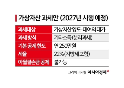 "Stocks Are Not Taxed, but Annual Crypto Gains Over 2.5 Million Won to Be Taxed Next Year... Investors Push Back"
- "Not Jealous of Winning the Lottery"... Entire Village Stunned as 200 Million Won Jackpot of Wild Ginseng Cluster Discovered at Jirisan
- "Even With a 90 Million Won Salary and Bonuses, It Doesn’t Feel Like Much"... A Latecomer Rookie Who Beat 70 to 1 Odds [Scientists Are Disappearing] ③
- "Rather Than Endure a 1.5 Million KRW Stipend, I'd Rather Earn 500 Million in the U.S." Top Talent from SNU and KAIST Are Leaving [Scientists Are Disappearing] ①
- "How Did an Employee Who Loved Samsung End Up Like This?"... Past Video of Samsung Electronics Union Chairman Resurfaces
To date, the Samsung Future Technology Development Program has supported 682 projects with 886.5 billion KRW. It has also shown active results with a total of 2,130 papers published in international academic journals. Among these, 189 papers have been featured in top-tier international journals such as Nature (7 papers), Science (7 papers), and Cell (1 paper).
© The Asia Business Daily(www.asiae.co.kr). All rights reserved.