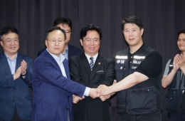
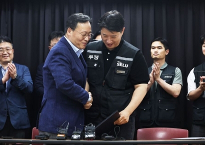
Hanul Materials Science: "HBM Advanced Packaging Materials as Next-Generation Growth Engine"
Hanul Materials Science announced on August 20 that it will foster high-bandwidth memory (HBM) advanced packaging materials as a next-generation core growth engine.

Hanul Materials Science has selected advanced packaging materials for hybrid bonding, which are virtually monopolized by Japanese companies, as a strategic item. These materials are considered the most optimized for hybrid bonding to date due to their excellent heat resistance, insulation properties, and low moisture content.
The HBM market is experiencing rapid growth as investments in data center servers related to artificial intelligence (AI) expand. Semiconductor companies are actively pursuing technology development and investment to secure leadership in the HBM market. Within the industry, packaging technology is being highlighted as a 'game changer' in the competition for dominance in the HBM sector. In particular, the development of hybrid bonding equipment and materials for the production of next-generation HBM with 16 or more layers is becoming increasingly important.
The company plans to gradually establish production facilities at its new Sejong plant while also securing specialized talent. Given the high technological entry barriers of these products, Hanul Materials Science also intends to establish cooperative systems with major conglomerates.
A representative from Hanul Materials Science stated, "With the rapid growth of the AI industry, semiconductor companies are significantly increasing their investments and efforts to secure HBM technology. As hybrid bonding technology for HBM packaging with 16 or more layers gains attention, the need for material development in addition to equipment is also rising."
The representative added, "As a company specializing in semiconductor materials for both front-end and back-end processes, HBM packaging materials represent a blue ocean market with high entry barriers but significant growth potential. This production initiative is aimed not only at responding to increasing industrial demand but also at contributing to supply chain stability through localization."
Hot Picks Today
 Up to 600 Million Won for Semiconductors, 160 Million Won Bonus for Loss-Making Non-Memory… Samsung Electronics Labor and Management Reach Tentative Deal on Unprecedented Performance Compensation (Comprehensive)
- "Could I Also Receive 370 Billion Won?"... No Limit on 'Stock Manipulation Whistleblower Rewards' Starting the 26th
- "From a 70 Million Won Loss to a 350 Million Won Profit with Samsung and SK hynix"... 'Stock Jackpot' Grandfather Gains Attention
- Opening a Bank Account in Korea Is Too Difficult..."It Costs 150,000 Won Just to Open a Child's Account or Check Card" [Foreigner K-Finance Status]②
- "Who Is Visiting Japan These Days?" The Once-Crowded Tourist Spots Empty Out... What's Happening?
Meanwhile, Hanul Materials Science is accelerating the establishment of facilities at its Sejong plant, aiming to obtain operational approval within the year. The company plans to develop this site into a 'total solution partner' production base, building a strategic portfolio that includes semiconductor photo process materials, HBM advanced packaging materials, and advanced heat dissipation film materials for data centers.
© The Asia Business Daily(www.asiae.co.kr). All rights reserved.