Samsung Electronics' New Foundry President: "Break the Vicious Cycle and Rebound with 2nm"
Hanjinman DS Division Foundry Business Unit Head's First Message
"We believe that we will be able to show a visible turnaround next year."
Han Jin-man, President of the Foundry Division at Samsung Electronics' DS Division, emphasized the rapid ramp-up of the advanced '2nm (nanometer, one billionth of a meter) process' as his first message after taking office on the 9th, stating, "I am confident that our division will grow to become Samsung Electronics' most important business unit in the near future."
In a message posted on the company bulletin board that day, President Han said, "Although we were the first to achieve the transition to the Gate-All-Around (GAA) process, there is still much lacking in commercialization," adding, "We must break the vicious cycle of having the window of opportunity close and having to take another gamble on the next node (such as 3nm, 2nm semiconductor process technology levels)." This was his first internal communication since his appointment as head of the semiconductor foundry through the executive reshuffle on the 27th of last month.

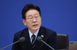
Hanjinman, President of the Foundry Business Division, Samsung Electronics DS Division. Photo by Samsung Electronics
View original imagePresident Han stated, "To achieve this, we must not only drastically improve process yield but also thoroughly identify every knob (Knob, optimization condition in semiconductor processes) to enhance PPA." PPA is a key metric in semiconductor manufacturing that evaluates Performance, Power efficiency, and Area. It is an essential standard to meet customer demands and develop competitive processes.
He said, "Mature node businesses are important as they can support the time and resources needed for the commercialization of advanced nodes," and urged, "Please focus on engineering activities to expand the commercialization of mature nodes developed by our division." He also emphasized, "We must devote all efforts to securing additional customers."
President Han also acknowledged the technological gap with competitors. He stated, "We must admit that our technology is lagging behind compared to other major companies." In fact, local media reported that TSMC recently achieved a test production yield exceeding 60% for its 2nm process products and plans to start mass production of 2nm process products from next year. Samsung Electronics developed the world's first 3nm semiconductor in March 2022, but its foundry market share declined from 18% in 2021 to 9.3% in the third quarter of this year.
However, President Han said, "We will overcome this someday," adding, "Although we cannot catch up with major foundry companies in the short term, let us find technological competitiveness so that those supporting sales and technology on the ground can confidently provide our foundry services."
Hot Picks Today
 "Stocks Are Not Taxed, but Annual Crypto Gains Over 2.5 Million Won to Be Taxed Next Year... Investors Push Back"
- "Don't Throw Away Coffee Grounds" Transformed into 'High-Grade Fuel' in Just 90 Seconds [Reading Science]
- Signed Without Viewing for 1.6 Billion Won... Jamsil and Seongbuk Jeonse Prices Jump 200 Million Won in a Month [Real Estate AtoZ]
- "Groups of 5 or More Now Restricted"... Unrelenting Running Craze Leaves Citizens and Police Exhausted
- "Even With a 90 Million Won Salary and Bonuses, It Doesn’t Feel Like Much"... A Latecomer Rookie Who Beat 70 to 1 Odds [Scientists Are Disappearing] ③
Finally, President Han called for improvements in inefficient work practices within the organization. He earnestly requested, "I sincerely ask business unit leaders to pay special attention to ensure that employees do not waste valuable time on unnecessary report writing or reporting," and urged, "Please allow engineers to spend more time experimenting and thinking."
© The Asia Business Daily(www.asiae.co.kr). All rights reserved.