Intel pouring money into foundries... Companies betting their survival on 'ecosystem expansion'
Intel's 'Aggressive Moves' Announce $1 Billion Fund Creation
Samsung Also Focuses on Ecosystem Development by Holding SAFE Forum Annually

[Asia Economy Reporter Lee Hye-young] Global semiconductor companies, heralding a "foundry (semiconductor contract manufacturing) showdown," are putting their lives on building ecosystems. Intel, which declared its re-entry into the foundry business, has launched a large-scale fund to secure an ecosystem and is chasing TSMC and Samsung Electronics.
Samsung Electronics, which has been focusing on creating a semiconductor ecosystem, plans to accelerate innovation in foundry and system semiconductors this year by strengthening cooperation with its partners.
On the 7th (local time), Intel's independent foundry division, IFS, and Intel Capital announced the establishment of a $1 billion (approximately 1.2 trillion KRW) fund to build a foundry innovation ecosystem. The fund will prioritize investments in areas that can accelerate the launch of intellectual property, software tools, innovative semiconductor architectures, and advanced packaging technologies.
Intel is expected to form partnerships with several companies affiliated with the fund to support next-generation advanced packaging processes and share technologies with customers. It also announced strategic industrial changes such as developing modular products with an open chiplet platform and expanding the scope of the open instruction set architecture (ISA) 'RISC-V' for chip design.
Pat Gelsinger, Intel's CEO, said, "The semiconductor design ecosystem is crucial to Intel's foundry division's success," adding, "Through the ecosystem fund and open chiplet platform, we will operate an ecosystem that can develop innovative technologies across chip architectures."
Intel also announced the launch of the foundry ecosystem called 'IFS Accelerator.' This aims to provide comprehensive support to smoothly carry out all semiconductor-related stages from design to execution and production.
Once the "absolute powerhouse" in semiconductors, Intel's status has declined as it struggled in its main central processing unit (CPU) field and fell behind in the technology competition speed race. Last year, it faced a crisis when it lost the title of "No. 1 semiconductor company" to Samsung Electronics.
As a countermeasure, Intel announced its re-entry into the foundry business with "IDM 2.0," deciding to invest a total of $40 billion by building foundry plants in Arizona and Ohio with $20 billion each. The U.S. government and Congress are also pushing a semiconductor support bill worth $52 billion, making massive funding visible.

The 'SAFE (Samsung Advanced Foundry Ecosystem) Forum 2021,' part of Samsung Electronics' initiative to build a foundry ecosystem, is being held online. (Photo by Samsung Electronics)
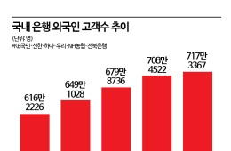
View original imageFoundry companies see the importance of building and expanding foundry ecosystems increasing as the "money war" intensifies. With technological advancement, adoption of cutting-edge processes, and rising design complexity intertwined, it becomes a decisive factor for foundry companies to attract as many fabless (design-specialized companies) as possible into their ecosystems for business success.
TSMC, a pioneer in foundry ecosystem creation, is also striving to secure the competitiveness of partner companies supporting customers' chip designs by building a VCA (Value Chain Aggregator).
Samsung Electronics has also been building its foundry ecosystem with a long-term perspective. In 2018, Samsung unveiled the 'SAFE (Samsung Advanced Foundry Ecosystem)' program to build a foundry ecosystem and has held forums annually since 2019 to share technology trends and strengthen cooperation.
Through this, Samsung Electronics provides partners with opportunities to explain and discuss essential solutions in semiconductor design and production, including EDA and IP, as well as cloud, design, and packaging fields. At the forum held last November, themed "Performance Platform 2.0," they discussed ways to strengthen solutions necessary for implementing chips based on cutting-edge processes and expanded infrastructure with partners.
Through this, they secured more than 80 EDA tools and technologies, including design infrastructure optimized for the 3nm GAA (Gate-All-Around) structure scheduled for mass production in the first half of this year, 2.5D and 3D package design solutions, and AI-based EDA.
Hot Picks Today
 Samsung Electronics Introduces New "Special Performance Bonus" for Semiconductors, Paid Entirely in Company Shares
- "Could I Also Receive 370 Billion Won?"... No Limit on 'Stock Manipulation Whistleblower Rewards' Starting the 26th
- "From a 70 Million Won Loss to a 350 Million Won Profit with Samsung and SK hynix"... 'Stock Jackpot' Grandfather Gains Attention
- Will Soaring Semiconductor Prices Support a Gradual Stabilization of the Household Debt Ratio? Why [BOK Focus]
- "Who Is Visiting Japan These Days?" The Once-Crowded Tourist Spots Empty Out... What's Happening?
Kim Yang-peng, a senior researcher at the Korea Institute for Industrial Economics & Trade, said, "For foundry companies to secure customers, building an ecosystem is very important," adding, "It is an essential requirement for global companies to choose foundries that secure as many design companies as possible and build a solid ecosystem sharing IP, which directly relates to foundry survival and competitiveness."
© The Asia Business Daily(www.asiae.co.kr). All rights reserved.