'Asia Semiconductor Technology Hub' ASML Completes Hwaseong Headquarters... Next-Generation Process Laboratory for Samsung and SK
240 Billion Won Invested in New Korean Headquarters
Samsung and SK Accelerate High-NA EUV Adoption
Engineer Training and Process Support Now Possible in Korea
ASML, the world's largest photolithography equipment manufacturer, has completed its new headquarters in Hwaseong, Gyeonggi Province, officially establishing South Korea as a core technology hub in Asia, following Taiwan. Designed as a "technology laboratory" equipped with advanced photolithography equipment operations, training, and remanufacturing functions, the facility is expected to directly enhance the next-generation microfabrication competitiveness of Samsung Electronics and SK Hynix.
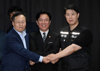
According to the industry on November 12, ASML will hold an opening ceremony for its new headquarters at the Dongtan General Industrial Complex in Hwaseong, Gyeonggi Province, on this day. Christopher Fooke, CEO of ASML, has traveled to Korea to attend the ceremony. Key technology executives from both companies, including Song Jaehyuk, Chief Technology Officer (CTO) and Head of the Semiconductor Research Center at Samsung Electronics, and Cha Sunyong, President and Head of the Future Technology Research Institute at SK Hynix, will also be present.

Aerial view of the new ASML headquarters located in Hwaseong, Gyeonggi Province. Ssangyong Construction.
View original imageASML invested a total of 240 billion won to construct this new headquarters, aiming to strengthen cooperation with domestic semiconductor companies such as Samsung Electronics and SK Hynix.
Headquartered in the Netherlands, ASML is the exclusive supplier of extreme ultraviolet (EUV) photolithography equipment. The new Hwaseong headquarters consists of three core areas: a remanufacturing center, a training center, and an experience center. Its significance lies in being a "technology complex hub," where advanced technology experiments and equipment operation training take place simultaneously, rather than simply serving as an office space.
Until now, the domestic semiconductor industry had to send engineers to the Netherlands headquarters or Taiwan for advanced photolithography equipment procurement and technical training. Now, education, repair, and verification can be conducted locally. An industry insider stated, "ASML is a crucial partner because it manufactures equipment essential for companies engaged in microfabrication," adding, "The new headquarters will provide a foundation for domestic semiconductor companies to collaborate with ASML more quickly and efficiently."
Hot Picks Today
 If They Fail Next Year, Bonus Drops to 97 Million Won... A Closer Look at Samsung Electronics DS Division’s 600M vs 460M vs 160M Performance Bonuses
- Opening a Bank Account in Korea Is Too Difficult..."Over 150,000 Won in Notarization Fees Just for a Child's Account and Debit Card" [Foreigner K-Finance Status]②
- Unable to Find Jeonse, Renters Pushed to Monthly Rent... Seoul Apartment and Villa Price Indices Hit Record Highs [Real Estate AtoZ]
- Room Prices Soar from 60,000 to 760,000 Won and Sudden Cancellations: "We Won't Even Buy Water in Busan" — BTS Fans Outraged
- "Who Is Visiting Japan These Days?" The Once-Crowded Tourist Spots Empty Out... What's Happening?
ASML first entered Korea in 1996 and established the ASML Korea headquarters and technical support center in Dongtan in 2016, but these primarily focused on customer support and sales functions. The new Hwaseong headquarters replaces the existing office and marks the first "advanced technology-type headquarters" with expanded scale and roles. With facilities for High-NA EUV photolithography equipment training, maintenance, and remanufacturing, it is expected to elevate Korea to ASML's core technology hub in Asia, following Taiwan.
© The Asia Business Daily(www.asiae.co.kr). All rights reserved.
!["Please Help Us": How Much Do Those Bowing 90 Degrees These Days Actually Earn? [Data Pick]](https://cwcontent.asiae.co.kr/asiaresize/307/2026052010120870131_1779239528.png)