'Under Construction' Samsung Secures First Official Order at US Taylor Plant... AI Chip Production Using 4nm Process
Korean AI Semiconductor Company 'Groke' Secures Clients
First Official Order for Taylor Factory to Open This Year
"4nm Yield Stable"... Diversifying AI Applications
Samsung Electronics' foundry (semiconductor contract manufacturing) division has secured a U.S. AI semiconductor company as a client, thanks to the stabilization of the 4-nanometer (㎚·one billionth of a meter) process yield. This is the first official order case for the Taylor plant in Texas, USA, which is scheduled to be completed within this year.
Grok announced on the 15th (local time) that it will produce its next-generation AI accelerator chip, the LPU (Latency Processing Unit), using Samsung Electronics' foundry 4-nanometer process. The company, founded in 2016 by former Google engineers, is a U.S.-based AI semiconductor design firm. It has introduced the LPU, a type of AI semiconductor equipped with an engine that maximizes memory bandwidth usage to perform inference computations at high speed.
Grok hinted that the product will be manufactured at Samsung's foundry plant being built in Taylor, Texas. This effectively makes it the first official customer of the Taylor plant. The Taylor plant is Samsung Electronics' second foundry facility in the U.S., following the Austin plant in Texas, and aims for completion within this year.
Earlier, Kyung Kye-hyun, President of Samsung Electronics' Device Solutions Division, revealed on his social media account that the AI boom is spreading globally and stated, "We will begin mass production of 4-nanometer process products at the Taylor plant from the end of 2024." He also explained, "Major U.S. customers expect their products to be manufactured here."

Samsung Electronics is currently expanding its market presence by increasing the yield (the ratio of good products among finished products) of the 4-nanometer process. In the semi-annual report released on the 14th, the company stated, "We are mass-producing the second-generation 4-nanometer products based on stable yields," and "The goal of mass production for the third-generation products in the fourth quarter is expected to be achieved." Market evaluations are also positive. Sangwook Park, a researcher at Hi Investment & Securities, estimated in a report last month that Samsung Electronics has raised the 4-nanometer process yield from the 50% range to recently about 75%.
Since this year, Samsung Electronics has also been providing 4-nanometer Multi-Project Wafer (MPW) services. MPW refers to the pilot production of various semiconductors on a single wafer in small quantities and multiple varieties. It is a mandatory step that fabless (semiconductor design) customers must go through before mass production. Industry insiders interpret Samsung Electronics' launch of MPW services as a sign of confidence in the 4-nanometer yield.
Samsung Electronics plans to target the high-growth AI semiconductor market based on its advanced fine process technology. At the 'Samsung Foundry Forum 2023' held last month, the company expressed its ambition to expand its AI-era business by leveraging next-generation Gate-All-Around (GAA) transistor technology and packaging technology. At the event, Samsung Electronics introduced success stories of its foundry customers and emerging AI semiconductor companies, Rebellion and DeepX.
Si-young Choi, President of Samsung Electronics Foundry Division, said, "The application areas of AI are rapidly expanding, and explosive growth is expected especially in edge computing specialized for various individual services." He added, "Samsung Electronics will lead the AI era paradigm through cutting-edge processes specialized for high-performance AI semiconductors, differentiated specialty processes, and close, proactive collaboration with global semiconductor intellectual property (IP) partners."

Interior view of the 'Samsung Foundry/SAFE Forum' held by Samsung Electronics on July 4 at COEX, Samseong-dong, Seoul / Photo by Samsung Electronics
View original imageMeanwhile, Samsung Electronics shared its foundry market outlook in this semi-annual report. Despite continued weak demand in the foundry market, the company stated, "We expect gradual recovery from the third quarter due to demand stimulation from AI-related high-performance computing demand, expanded applications, increased smartphone demand, and supply chain normalization." It also forecasted, "In the mid to long term, growth will continue due to sustained mobile demand and increased demand for high-performance SoCs (autonomous driving) for automotive applications."
Hot Picks Today
 "Could I Also Receive 370 Billion Won?"... No Limit on 'Stock Manipulation Whistleblower Rewards' Starting the 26th
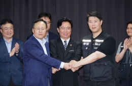
- Samsung Electronics Labor-Management Reach Agreement, General Strike Postponed... "Deficit-Business Unit Allocation Deferred for One Year"
- "From a 70 Million Won Loss to a 350 Million Won Profit with Samsung and SK hynix"... 'Stock Jackpot' Grandfather Gains Attention
- "Stocks Are Not Taxed, but Annual Crypto Gains Over 2.5 Million Won to Be Taxed Next Year... Investors Push Back"
- "Who Is Visiting Japan These Days?" The Once-Crowded Tourist Spots Empty Out... What's Happening?
To prepare for the market situation transitioning to a foundry growth phase, the company is focusing on improving the maturity of the GAA-based 3-nanometer process and expanding production capacity through new plants. Going forward, it said, "We will continuously improve cost competitiveness through process technology improvements and expansion of high-margin products," and "We will pursue portfolio diversification by application, including high-performance computing, automotive semiconductors, 5th generation mobile communications (5G), and Internet of Things (IoT)."
© The Asia Business Daily(www.asiae.co.kr). All rights reserved.