[Photo] Samsung Electronics Ships First 3nm Foundry Mass Production Products
![[Photo] Samsung Electronics Ships First 3nm Foundry Mass Production Products](http://www.asiae.co.kr/news/img_view.htm?img=2022072510430562231_1658713385.jpg)
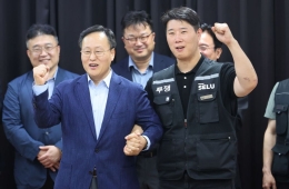
On the 25th, at the world’s first GAA-based 3nm mass production shipment ceremony held at Samsung Electronics Hwaseong Campus in Hwaseong-si, Gyeonggi Province, Lee Chang-yang, Minister of Trade, Industry and Energy, and Kyung Kye-hyun, CEO of Samsung Electronics, along with other attendees, shouted "Fighting." The 3nm process is the most advanced technology among semiconductor manufacturing processes, and GAA is also known as a next-generation core technology that enhances semiconductor efficiency through precise control. / Hwaseong = Reporter Kim Hyun-min kimhyun81@
Hot Picks Today
 If They Fail Next Year, Bonus Drops to 97 Million Won... A Closer Look at Samsung Electronics DS Division’s 600M vs 460M vs 160M Performance Bonuses
- Opening a Bank Account in Korea Is Too Difficult..."Over 150,000 Won in Notarization Fees Just for a Child's Account and Debit Card" [Foreigner K-Finance Status]②
- Whistleblowers Could Earn Tens of Billions by Reporting Collusion... KFTC Announces Administrative Notice to Abolish Reward Cap
- Room Prices Soar from 60,000 to 760,000 Won and Sudden Cancellations: "We Won't Even Buy Water in Busan" — BTS Fans Outraged
- "Who Is Visiting Japan These Days?" The Once-Crowded Tourist Spots Empty Out... What's Happening?
This content was produced with the assistance of AI translation services.
© The Asia Business Daily(www.asiae.co.kr). All rights reserved.
!["Please Help Us": How Much Do Those Bowing 90 Degrees These Days Actually Earn? [Data Pick]](https://cwcontent.asiae.co.kr/asiaresize/307/2026052010120870131_1779239528.png)