Samsung Electro-Mechanics Participates in Korea's Largest Substrate Exhibition

Samsung Electro-Mechanics Participates in International Printed Circuit Exhibition 2020
View original image[Asia Economy Reporter Changhwan Lee] Samsung Electro-Mechanics announced that it will participate in the '2020 KPCA Show Exhibition (International Electronic Circuit and Mounting Industry Exhibition)' held for three days from the 24th to the 26th at Songdo Convensia, Incheon.
Marking its 17th year, the KPCA Show is the largest domestic circuit board exhibition, attended by domestic and international substrate manufacturers as well as material and equipment companies.
Samsung Electro-Mechanics showcased various substrate solutions, including advanced semiconductor package substrates and SiP (System in Package) module substrates, to respond to the high performance demands of electronic devices.
Samsung Electro-Mechanics exhibited products categorized into Advanced Solutions and IT Solutions according to substrate types and technologies.
In Advanced Solutions, numerous products were displayed to address the high performance and slimming of semiconductors for 5G communication, AI (Artificial Intelligence), and automotive electronics.
In particular, antenna substrates essential for ultra-high-speed 5G communication integrated antennas and RF modules into printed circuit boards, improving high-frequency signal sensitivity and reducing size.
They also exhibited high-density package substrates embedding passive components such as MLCC (Multilayer Ceramic Capacitors) into substrates, advantageous for high-speed signal transmission and applicable to AI accelerators and automobiles.
In IT Solutions, semiconductor substrates applied to smartphones, PCs, and more were introduced. The FCCSP (Flip Chip Chip Scale Package), a package substrate applied to mobile application processors (AP), featured differentiated circuit pattern shapes and exhibited an ultra-slim product with thickness reduced by 40% compared to existing ones.
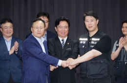
Meanwhile, at the electronic circuit industry development merit award ceremony held on the opening day, Kim Eungsu, Head of the Substrate Manufacturing Team (Executive Director), will receive the Minister of Trade, Industry and Energy Award.
Executive Director Kim received the award for his achievements in developing and mass-producing the first domestic package substrates for central processing units (CPU) and graphics processing units (GPU), and securing ultra-fine circuit implementation technology through the development of core materials related to semiconductor substrates.
Hot Picks Today
 "Could I Also Receive 370 Billion Won?"... No Limit on 'Stock Manipulation Whistleblower Rewards' Starting the 26th
- Samsung Electronics Labor-Management Reach Agreement, General Strike Postponed... "Deficit-Business Unit Allocation Deferred for One Year"
- "From a 70 Million Won Loss to a 350 Million Won Profit with Samsung and SK hynix"... 'Stock Jackpot' Grandfather Gains Attention
- "Stocks Are Not Taxed, but Annual Crypto Gains Over 2.5 Million Won to Be Taxed Next Year... Investors Push Back"
- "Who Is Visiting Japan These Days?" The Once-Crowded Tourist Spots Empty Out... What's Happening?
Executive Director Kim Eungsu said, “I am very pleased that this award recognizes Samsung Electro-Mechanics' contributions and significance in the semiconductor package substrate industry. We will continue to strive tirelessly to establish technological competitiveness that leads the global industry.”
© The Asia Business Daily(www.asiae.co.kr). All rights reserved.